Hmm, gotta think about this.
First impressions:
#1 Only if the first stage is a source follower will there be no phase reversal
#2 Grounded base needs constant current to deliver good linearity
#3 There is no feedback in this circuit to deliver the necessary low Zout and distortion
#4 Output is single ended, not push pull, therefore Class A with commensurate low power
#5 Jfet selection required to deliver appropriate operating point
#6 Miller cap would be difficult to implement because no phase reversal at the VAS
#7 There will be inevitable phase shift, like any other amplifier, from input to output
Hugh
SWF:
Yes that is what i thought too. The oscillation is in the negative voltage swing.
Hugh:
You cannot build an amp that does have 100% identical positive and negative slew-rate. And it is the nature of this circuit layout. I have no problem with it,
Keantoken:
Is it not better to be more pessimistic then optimistic!?
If one build a better quality board layout with low parasitic inductance, don't you think that the circuit should be stable too in this layout as well as in an sluggish layout!?!?!?
I did this to be able to follow up on this thread (Which has a very very high pace at the moment). I do not think that it is a bad circuit and it is easy to stabilize. One way of doing it was to modify the feedback loop as shown.
Hugh,
That´s an overall description of the common base amplifier not a description of that particular circuit.
Only the common emitter / source / cathode configuration introduces a 180 degree phase inversion, not to be confused with phase displacement.#1 Only if the first stage is a source follower will there be no phase reversal
All topologies do. Constant DC values are a condition of linear function.#2 Grounded base needs constant current to deliver good linearity
The circuit is not adapted, meant for demonstration purposes only.#3 There is no feedback in this circuit to deliver the necessary low Zout and distortion
#4 Output is single ended, not push pull, therefore Class A with commensurate low power
It´s always the case with J-FETs.#5 Jfet selection required to deliver appropriate operating point
There are many ways to accomplish phase compensation.#6 Miller cap would be difficult to implement because no phase reversal at the VAS
Certainly so.#7 There will be inevitable phase shift, like any other amplifier, from input to output
That´s an overall description of the common base amplifier not a description of that particular circuit.
Sonnya, if SWF prefers to leave the circuit without compensation, then construction will mess with stability no matter what. This is one of the trade-offs with having no compensation... It is up to the builder to find a layout that works, if he is not comfortable with the original one.
- keantoken
- keantoken
Hi WuYit,
OK, you understand the limitations. Problem is, if you suggest something new, it's best to deliver a schematic that actually improves on the existing circuit, which our SWF is valiantly attempting to do. I think your post is a little discouraging, and I strive to foster SWF's efforts in this thread.
You clearly have all the advantages/disadvantages in your mind, but your circuit was rather simplistic.
Incidentally, I have built a grounded base VAS, and if you use a LTP the phase issue is a non-event, including the compensation. But in your circuit, about the only way you could implement LC would be via shunt, which is a bit compromised. The other option is to use a bootstrap with a lousy, highly inductive cap, to pull back loop gain by the upper pole.
I have always felt that a successful audio amp design is the artful management of compromise, and that the measure of excellence may not necessarily be a number, THD or otherwise. As a group, we diyers really are hung up on the psychology of numerical appraisal.
I should be clear that I'm not trying to poke fun at your circuit, but it was too simple to meaningfully contribute. Mind you, I can't talk, I'm not contributing anything on the forum, although I do speak to Greg off air. He's taking a well earned break, BTW!
Cheers,
Hugh
I have always felt that a successful audio amp design is the artful management of compromise,
and that the measure of excellence may not necessarily be a number, THD or otherwise.
As a group, we diyers really are hung up on the psychology of numerical appraisal.
A compromise ..
Not numbers ..
I think you are very right, AKSA.
One thing this thread have teached me
is the sane topology importance.
Secondly a good selection of parts values comes before SPICE numbers.
If I was to build Fetzilla, it is not max lowest THD that should guide me,
but to have no or very moderate compensation capacitance.
Regards
Sonnya, if SWF prefers to leave the circuit without compensation, then construction will mess with stability no matter what. This is one of the trade-offs with having no compensation... It is up to the builder to find a layout that works, if he is not comfortable with the original one.
- keantoken
You don't get it... do you?
I am not trying to get him change his circuit. I was only giving my idear on how he could remove the oscillation.
As i stated: I am not sending it to the graveyard!
Sonnya, thanks for clarifying. Why not just put a 500R resistor in series with the phase lead cap and not mess with the series feedback resistor?
Your way puts a 100pF+150R network between the input and output of the output stage. I'm not sure if this is doing anything but increasing the load on the VAS.
- keantoken
Your way puts a 100pF+150R network between the input and output of the output stage. I'm not sure if this is doing anything but increasing the load on the VAS.
- keantoken
Actually, Kean, increasing the (resistive) load on the VAS tends to exploit its asymmetry and create higher levels of H2 and H3. Some people like this; it sounds tubey.
I agree about messing with the series feedback resistor. I've found that even small caps across this can actually reduce stability because of the additional phase shift in the output stage.
Hugh
I agree about messing with the series feedback resistor. I've found that even small caps across this can actually reduce stability because of the additional phase shift in the output stage.
Hugh
progress report
I am building boards using blank vero board, pins & copper wire, one finished the other 1/2 done, these will be great for experimentation but are a labour of love to build. Have to test & match some components now. As you can see I'm not rushing but should have one working cct in a few days.
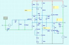
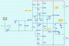
The number of versions bouncing around here is enough to make a potential builder giddy but initially I'm interested to two versions only and I thought I would see what the experts think about how they compare theoretically. They differ only in VAS. 1) irf9610 2) casoded bd140s
Earlier in the thread a BJT VAS was discarded due to lack of OLG ( about 75dB ) but if a cascode is added the gain increases to almost 100dB which is flat to about 1Khz which with my CLG target of 20 - 24 dB should be plenty of FB.
Many here have stated that they prefer a BJT for VAS and I think the cascode makes it a viable contender.
In simulation I saw advantages in keeping the VAS current high so I'm begining with 20mA. I would be interested in alernative device suggestions.
My new PC scope arrived today which is great but I can tell you that building when all your usual parts, tools & testing gear are on a boat on the Atlantic is quite a challenge !
I am building boards using blank vero board, pins & copper wire, one finished the other 1/2 done, these will be great for experimentation but are a labour of love to build. Have to test & match some components now. As you can see I'm not rushing but should have one working cct in a few days.
The number of versions bouncing around here is enough to make a potential builder giddy but initially I'm interested to two versions only and I thought I would see what the experts think about how they compare theoretically. They differ only in VAS. 1) irf9610 2) casoded bd140s
Earlier in the thread a BJT VAS was discarded due to lack of OLG ( about 75dB ) but if a cascode is added the gain increases to almost 100dB which is flat to about 1Khz which with my CLG target of 20 - 24 dB should be plenty of FB.
Many here have stated that they prefer a BJT for VAS and I think the cascode makes it a viable contender.
In simulation I saw advantages in keeping the VAS current high so I'm begining with 20mA. I would be interested in alernative device suggestions.
My new PC scope arrived today which is great but I can tell you that building when all your usual parts, tools & testing gear are on a boat on the Atlantic is quite a challenge !
Mikelm,
Great to see you're making progress.....my guess is you will prefer the 9610.
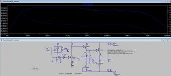
Can someone please explain to me how to test stability with spice? I have run an ac analysis on my circuit and get a nice decrease at HF on the ouput node. The only place I see an increase is at the gate to the VAS, which I assume is bad?
I have also tried a square wave with 10us on, 20uS period and rise and fall times of 10nS. I can not get the thing to oscillate in simulation - Sonnya, what am I doing wrong?
Great to see you're making progress.....my guess is you will prefer the 9610.
Can someone please explain to me how to test stability with spice? I have run an ac analysis on my circuit and get a nice decrease at HF on the ouput node. The only place I see an increase is at the gate to the VAS, which I assume is bad?
I have also tried a square wave with 10us on, 20uS period and rise and fall times of 10nS. I can not get the thing to oscillate in simulation - Sonnya, what am I doing wrong?
SWF,
Set input siggen to 0V input.
Insert AC voltage source between output and the series fb resistor. Set AC voltage to 1 on the LTSpice right side of the dialogue box. (Left side should be left at zero).
Right of the AC voltage source is Vout; label left of the voltage source Vb by right clicking on the line input to the voltage source.
Select Functions NONE and AC Amplitude 1 (to the upper right) after right clicking on the AC voltage source.
Choose Edit Simulation Command, and then select AC Analysis.
Specify a frequency range from 10Hz to 20MHz. This covers the areas of interest of all audio amplifiers.
Now, run the simulation.
Right click the empty plot to add a trace. Insert the following function: -Vout/Vb
You will then see a plot of loop gain (OLG/CLG) for the frequencies selected. This is Middlebrook Analysis. On a typical amp you will see loop gain start to drop from the dominant pole, around 2Khz or so. At the point where the loop gain has dropped exactly 3dB, this is a 45 degree phase shift, and gives the dominant pole (lower). This value is significant as it tells you exactly where the loop gain starts to reduce with increasing frequency. It would be nice to have this frequency above the audio band, but it almost never is.
Now, look at the broken line, which represents phase shift of the -Vout/Vb function. At the point where phase shift is exactly 180 degrees displaced, we have negative feedback changing abruptly into positive feedback. Normally this phenomenon leads to destructive oscillation. At this exact point, trace the gain from the curve. It should be well below 0dB loop gain. If this is so, the amp is stable.
A useful refinement is to examine the phase margin at the point where loop gain is 0dB. Phase margin is the safety factor; it is 180 minus the precise phase shift at that point. If the phase shift is, for example, 100 degrees at loop gain of 0dB, then phase margin is 80 degrees, which is pretty good. However, to reduce your phase margin, push the limits by placing a parallel cap across the 8R resistive load on the amplifier. The worst cap I've found for testing phase margin is 100nF.
On my amp, the NAKSA, 0dB loop gain occurs at 545KHz, with 85 degrees of phase margin. Dominant pole is at 23.5KHz.
Hope this explains it,
Hugh
Last edited:
Hugh,
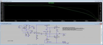
Thanks again, how's this one? Found an example in the examples folder of lt spice!
Not entirely sure what this is actually doing. Might be a good topic next time we speak on the phone!
P.S. don't pay too much attention to the actual schematic. I'm just trying to get the stability testing sorted. The vas is actually at 10mA.
Attachments
Last edited:
- Status
- This old topic is closed. If you want to reopen this topic, contact a moderator using the "Report Post" button.
- Home
- Amplifiers
- Solid State
- JFET input, MOSFET VAS, LATERAL output = Perfect!!