Stability issue I'd guess. Same with why it drops when you touch it I think you said. Look with a scope...
No thoughts on what might cause the strange DC offset drop at 7 minutes? Is this kind of thing normal?
Very glad to see how stable it eventually turned out to be though.
About the ZVN3310 and the ZVP3310.
VGS versus ID WILL change over temperature, even if the datasheet does not show variation over temperature.
The ZVP3310 in the top, is connected to a current source. So to optain balance voltage in the VAS stage, the vgs of the ZVP3310 will be floating until it has settled at a fixed temperatur..
The only way to compensate for the changing VGS voltage is to get the ZVN3310 in the inputstage to draw more or less current. It is connected to a currentsource - So the current can only be drawn from you feedback resistor. So the current through the 1K feedback resistor changes - There you have your drift.
Try cool the ZVP3310 in the vas stage with a cooling spray and see what happend!?
Last edited:
Hmm, thanks that's an interesting idea. Will try it tonight. I also think the issue has to be thermal, I just wouldn't have expected such a sudden change. I'm actually thinking about trying the quasi version now so I can drop the current in the VAS to just a few mA.
Hugh, glad you're back - I've sent you an email.
Hugh, glad you're back - I've sent you an email.
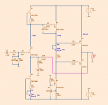
Fetzilla, recommended.
Below is the Fetzilla how I think it should be.
Like an official version.
Most surely you will make your own version.
But as a guide you can go back to this official version.
It does run in Class AB bias 100 mA.
You can bias harder, in Class A, if you like.
To build you need:
- One Transformer 2x18VAC, 100VA or more. Gives ~2x25VDC
- 3 JFETs, preferably 2SK170BL
- 2 MOSFETs, ZVP3310A,ZVN3301A
- 1 BC550 or similar small signal transistor
- 2 Lateral Mosfets, 2SK1058, 2SJ162
- 2 Trimpotentiometers
Enjoy")
Below is the Fetzilla how I think it should be.
Like an official version.
Most surely you will make your own version.
But as a guide you can go back to this official version.
It does run in Class AB bias 100 mA.
You can bias harder, in Class A, if you like.
To build you need:
- One Transformer 2x18VAC, 100VA or more. Gives ~2x25VDC
- 3 JFETs, preferably 2SK170BL
- 2 MOSFETs, ZVP3310A,ZVN3301A
- 1 BC550 or similar small signal transistor
- 2 Lateral Mosfets, 2SK1058, 2SJ162
- 2 Trimpotentiometers
Enjoy
Attachments

mmm - I think that before we can recommend this design as "official" we have have someone confirm that it works in real life.
People could interpret "official" as "tested & reliable with different types of load" and personally I have a few doubts about this - especially with the extra open loop gain added with the CCS as input load resistor
People could interpret "official" as "tested & reliable with different types of load" and personally I have a few doubts about this - especially with the extra open loop gain added with the CCS as input load resistor
Mike,
I think I agree, OTOH Lineup's design is a good one, an excellent start point.
Personally, I have always had misgivings about trimming the offset with a CCS in the source of the input device. I would prefer to see this device pass its entire output through the feedback resistor, and the gate biased to an appropriate voltage to achieve null ouput offset.
Further, I'm not sure I much favor the use of a CCS on the drain of the input jfet. Since using both a jfet and a mosfet VAS is intended to deliver a square law transfer function and for reasons of low transconductance a much lower loop gain, say no more than 50dB, then a CCS loaded drain goes against this principle and actually elevates loop gain by at least 6dB. Only a resistively loaded drain, and a degenerated VAS will lower loop gain, which has palpable sonic benefits because the long trail of distortion artefacts, though higher in amplitude, is much shorter.
A mental exercise is very different to a finished, working amp. Even then, you have to build ten of them to guarantee they all work identically, since tolerances, particularly with FETs, are a fact of life.
Nearly there, however, not to be negative.....
Hugh
Lumba,
The cascode has disadvantages:
1. While it lowers distortion, it does NOT improve the sound (I've verified this empirically).
2. It is not needed with a rail voltage of just 25, since Vds is rated well above this voltage.
3. Zout, and thus drive, is not as good as a resistively connected drain.
4. It adds one further active device, and attendant bias networks.
In fact, if we were to add a cascode, it should be constant power cascode, where the cascode hikes up and down with the input signal, keep Vds constant across the input/feedback device.
Lastly, if we use a SE cascoded input stage as you suggest, then it would have to be cap coupled to drive a common source output stage. Cap coupling within a SS amplifier is less than desirable. There are ways around this, but they are wacky too.
No, I feel the amp should be left pretty much as is, though with the CCS below the jfet source omitted.
I support Mike's comments about offset. People are very concerned about it, but even at 200mV of offset, a high figure by the exacting standards of folks here, the voice coil DC dissipation is a miserable 5.8mW. Most speakers are designed to dissipate at least 25W continuously, so this is a walk in the park in broad daylight..... no, what is more important is the displacement of the cone with a bit of standing DC voice coil current. What does it do? Increase even, low order distortion, that's all - you wouldn't notice it in a million years of listening.
Kapitz?
Hugh
Last edited:
Most speakers are designed to dissipate at least 25W continuously, so this is a walk in the park in broad daylight.....
yes
funny tho that the low voltage single jfet was my immediate worry too
it won't be long until people ask for double outputs and more power
Another variation
All,
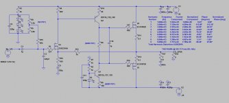
Edit: The schematic has an error. I am currently using no output zobel or snubber of any kind. The amp seems stable enough without it.
Taking some of master Hugh's advice on board, I have created the best incarnation of this amplifier I have heard yet. It appears stable, and DC offset appears predictable and manageable. Better yet we have dropped several active devices to do it. Note the minuscule distortion figures at 16V p2p into 8R. Hugh will also be happy that the low order harmonics taper off in ascending order
The modifications are all things Hugh quietly suggested way back in the thread.
As my JFETs have not yet arrived I am stuck with the mosfet front end and parts I had lying around. The bias scheme shown may have to be modified to allow a negative gate bias if a jfet is used. If there is enough interest I can post a schematic for biasing a jfet.
I have used resistor values I had at hand and the cheapest of cheap transistors. I think the circuit could be significantly improved and tweaked, but here is a good starting point. The jfet front end will work wonders, too.
The amp as it stands sounds very different to how it did before. The warmth that was in my initial version with the bootstrap VAS has come back. If you like valves this is the version to build. If you want detail, the last version I posted with the fet vas and bjt referenced CCS is the way to go. That said, my VAS may be getting let down by the poor parts I have used.
The amp seems stable and sounds very very nice. If you listen to easy going vocals you're in for a treat. A Dave Gilmour solo can sound pretty good too
All,
Edit: The schematic has an error. I am currently using no output zobel or snubber of any kind. The amp seems stable enough without it.
Taking some of master Hugh's advice on board, I have created the best incarnation of this amplifier I have heard yet. It appears stable, and DC offset appears predictable and manageable. Better yet we have dropped several active devices to do it. Note the minuscule distortion figures at 16V p2p into 8R. Hugh will also be happy that the low order harmonics taper off in ascending order
The modifications are all things Hugh quietly suggested way back in the thread.
As my JFETs have not yet arrived I am stuck with the mosfet front end and parts I had lying around. The bias scheme shown may have to be modified to allow a negative gate bias if a jfet is used. If there is enough interest I can post a schematic for biasing a jfet.
I have used resistor values I had at hand and the cheapest of cheap transistors. I think the circuit could be significantly improved and tweaked, but here is a good starting point. The jfet front end will work wonders, too.
The amp as it stands sounds very different to how it did before. The warmth that was in my initial version with the bootstrap VAS has come back. If you like valves this is the version to build. If you want detail, the last version I posted with the fet vas and bjt referenced CCS is the way to go. That said, my VAS may be getting let down by the poor parts I have used.
The amp seems stable and sounds very very nice. If you listen to easy going vocals you're in for a treat. A Dave Gilmour solo can sound pretty good too
Attachments
Last edited:
Nice and simple circuit. Clean and easy to understand.
THD 0.005 is low and typical for a well built version.
Hard to make it lower using so simple amplifier.
I wait for you to get JFET.
Will be interesting to see what you will come up with.
And I would use a Zobel: 47nF + 10 Ohm
Just in case.
Does not hurt or effect any sound.
THD 0.005 is low and typical for a well built version.
Hard to make it lower using so simple amplifier.
I wait for you to get JFET.
Will be interesting to see what you will come up with.
And I would use a Zobel: 47nF + 10 Ohm
Just in case.
Does not hurt or effect any sound.
Nice and simple circuit. Clean and easy to understand.
THD 0.005 is low and typical for a well built version.
Hard to make it lower using so simple amplifier.
I wait for you to get JFET.
Will be interesting to see what you will come up with.
And I would use a Zobel: 47nF + 10 Ohm
Just in case.
Does not hurt or effect any sound.
Thank you lineup. Yes you're correct, some sort of rc zobel would be prudent. I just wanted to demonstrate how stable the amplifier appears to be. This is a far cry from my initial build which I could not get to settle down.
I am very happy with it in this form. Sounds good and square wave response is spectacular as the higher dissipation of the bd transistors has allowed me to add another 5ma of vas current (total 15ma or so). On first impression dc offset is much more stable too. All in all there's a lot of bang for your buck - enviable performance for only a few $$ worth of parts. I built this current design on a perfboard in under an hour.
Last edited:
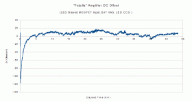
DC Offset Results
All,
DC offset results for the new circuit are in, and you're going to be very happy. These are a worst case scenario. They were taken using an unprotected circuit on a perfboard in a drafty room. Temperatures inside were warm and cold gusts were blowing in the window throughout the test. Temperature variation of the components is expected to be significant.
Hugh suggested removing the input ccs and biasing the fet gate with LEDs when the thread was in its infancy, but I didn't try it at the time as I didn't think such a simple circuit could work so well. I was wrong.
Turn on "thump" is only 120mV or so, much better than the 500mV of the original circuit. Offset drops to under 100mV almost instantly, and to within 20mV in a couple of minutes. It then easily stays within 15mV for the remainder of the test (total test time = 50min). The small scale deviations are higher in frequency than the original circuit, but the overall long term stability is better....and this is with two less active devices.
Attachments
Last edited:
- Status
- This old topic is closed. If you want to reopen this topic, contact a moderator using the "Report Post" button.
- Home
- Amplifiers
- Solid State
- JFET input, MOSFET VAS, LATERAL output = Perfect!!