Lineup,
Thank you for your replies and help so far. It's looking good I think. I have added the input filter. Still trying to get the lateral models to work.
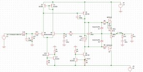
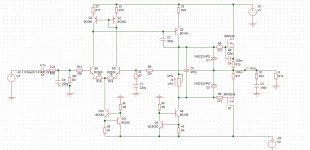
In the meantime I have been thinking that the VAS might be best made with a BD139 and BD140 (see below). The advantage of these over the ZVP3310 is that they can safely dissipate 0.5W without heatsinks which lets me increase the VAS current to 15mA.
I found that this configuration simmed worse than the fet CCS at 2kHz, but was better at 20kHz. The amp also seems a little bit more stable with the BJT VAS.
I have added C5 as per Hugh's schematic. This improved the THD at 20kHz too.
I have also added some current protection zeners which will be selected to limit the current to 10A or so.
One problem I have is that the simulated DC offset is now nearly 100mV. Any ideas for fixing that?
If you like I can send you the simetrix model of this amplifier.
Simetrix is a free simulator package for private use and comes with hundreds of models included. It can be downloaded from the simetrix website.
Thank you for your replies and help so far. It's looking good I think. I have added the input filter. Still trying to get the lateral models to work.
In the meantime I have been thinking that the VAS might be best made with a BD139 and BD140 (see below). The advantage of these over the ZVP3310 is that they can safely dissipate 0.5W without heatsinks which lets me increase the VAS current to 15mA.
I found that this configuration simmed worse than the fet CCS at 2kHz, but was better at 20kHz. The amp also seems a little bit more stable with the BJT VAS.
I have added C5 as per Hugh's schematic. This improved the THD at 20kHz too.
I have also added some current protection zeners which will be selected to limit the current to 10A or so.
One problem I have is that the simulated DC offset is now nearly 100mV. Any ideas for fixing that?
If you like I can send you the simetrix model of this amplifier.
Simetrix is a free simulator package for private use and comes with hundreds of models included. It can be downloaded from the simetrix website.
Attachments
I understand.
With BD139/140 you are free to experiment with different current in VAS.
With laterals you need not more than 5mA VAS.
With IRFP240/9240 I think it is very good with at least 10mA VAS.
So, for IRFP240/9240 I have used IRF610/9610 MOSFET for VAS.
This allows higher current.
15mA would not hurt for laterals. But is not needed.
Simetrix I have not tried.
I will have a look at it.
DC-offset.
In this kind of input you should put emitter resistors in the mirror at top.
For 5mA each take 22 Ohm resistors.
Because drop should be 100-200mV across those.
In a real circuit without emitter resistors there can be temperature with offset.
This AKSA said in a topic.
Usually I put a suitable resistor across Q1+Emitter resistor to achieve near zero offset.
Can be a potentiometer.
Last edited:
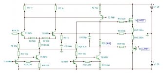
Output offset is due to the choice of resistors around the input.
Q8 base sees 2k2 + [220p//47k] if the input is DC blocked.
Q9 base sees 11k.
They don't match !!!!!!
If the input is not blocked, then
Q8 base sees 4k4. Still not matched.
The input offset current must be low. Q8 & Q9 must be Cgrade and preferably matched for Vbe and approximately matched for hFE. The simulation will assume that the LTP is exactly matched for Vbe and for hFE.
Input resistance seen by the input currents must be almost exactly matched. A slight offset current can be compensated by a slight adjustment of base resistance to ground.
Power amps perform better if the "impedance" seen by the input is very low.
R13 prevents that low impedance of the 220pF being seen.
Try reducing R13 to 200r or somewhere <<1k0. Some designers adopt 0r0.
If you increase R15 then C6 can be made a bit higher, reducing the base impedance a bit more.
C2 (Cdom) is too high. Add in LTP emitter resistors to lower the gain of the front end.
Read Cordell. Or look at how many "good" designs always include emitter degeneration.
Add degeneration to the VAS as well.
Last edited:
Output offset is due to the choice of resistors around the input.
Q8 base sees 2k2 + [220p//47k] if the input is DC blocked.
Q9 base sees 11k.
They don't match !!!!!!
yes, of course!
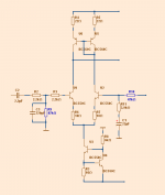
I show what your input could look like
when get zero DC-offset.
I added 10 Ohm emitter resistors to input pair
and 22 Ohm emitter resistors in mirror pair.
The main thing is that R9 and R10 are equal in value
because only those two gives base DC current to input pair.
Keeping them same value will give small DC-offset.
when get zero DC-offset.
I added 10 Ohm emitter resistors to input pair
and 22 Ohm emitter resistors in mirror pair.
The main thing is that R9 and R10 are equal in value
because only those two gives base DC current to input pair.
Keeping them same value will give small DC-offset.
Attachments
Lineup, Andrew,
Thanks for your help. I really appreciate it.
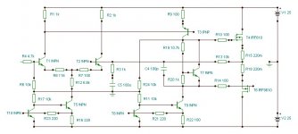
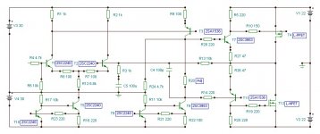
I added the degeneration to the mirror, LTP and VAS as you suggested. Simulated distortion doubled, but I guess it will help when the transistors are not equally matched (for the real life amplifier).
However, because of the reduced gain I was able to decrese the miller compensation cap which improved THD a bit.
Lineup, I tried changing the resistors on either side of the LTP to the values you suggested, but the offset went much higher! Instead, I tried decreasing the values of the feeback resistors which helped considerably. Only 3mV of offset now.
Also increased the input filter cap as Andrew suggested and dropped R13 to 200R.
Andrew, could you possibly explain how I determine the overall input impedence of the circuit?
Here is the current circuit. What do you think?
Thanks for your help. I really appreciate it.
I added the degeneration to the mirror, LTP and VAS as you suggested. Simulated distortion doubled, but I guess it will help when the transistors are not equally matched (for the real life amplifier).
However, because of the reduced gain I was able to decrese the miller compensation cap which improved THD a bit.
Lineup, I tried changing the resistors on either side of the LTP to the values you suggested, but the offset went much higher! Instead, I tried decreasing the values of the feeback resistors which helped considerably. Only 3mV of offset now.
Also increased the input filter cap as Andrew suggested and dropped R13 to 200R.
Andrew, could you possibly explain how I determine the overall input impedence of the circuit?
Here is the current circuit. What do you think?
Attachments
Thanks Lineup. Does this mean the amplifier can't be direct coupled?
Edit: now I know what you mean. I need to disconnect the generator!
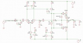
Wuyit, thanks for your design. Can you please exaplain why you think it is better? I see you have removed the current mirror and used a Vbe multiplier for the bias. Is there anything else that makes it special?
Edit: now I know what you mean. I need to disconnect the generator!
Wuyit, thanks for your design. Can you please exaplain why you think it is better? I see you have removed the current mirror and used a Vbe multiplier for the bias. Is there anything else that makes it special?
Last edited:
Even if your circuit does not need a capThanks Lineup. Does this mean the amplifier can't be direct coupled?
Edit: now I know what you mean. I need to disconnect the generator!
there will 90% sure be an output capacitor in what you connect to the input.
To keep gear from upsetting DC-offset it is good to put a cap on input of amplifier.
Not to would give a chance of upsetting DC-offset.
swordfishy,
without thermal compensation you may lose those FETs within seconds. Current mirror can be a good thing when implemented "right". I personally prefer to keep the open-loop gain low.
Wuyit,
My (poor) understanding is that at the bias currents I will be running (1A) with the lateral output fets I will be using (don't mind the schematic, I don't have lateral models), the tempco is negative, and therefore an increase in temp will reduce current. Please correct me if I'm wrong.
You can read about the lateral fets I will be using in an earlier post in this thread.
As for the current mirror, you may be right. The amp seems quite unstable and needs a large miller cap for stability. I might try simming a few circuits with a simple resistive load. Reduced OLG might really help in this regard. I hate oscillation!
Will try a few simulations and report back.
Wuyit,
Thank you for your updated schematic. I did a simulation and the amp was indeed more stable. I was able to drop the miller cap to 50pf. THD increased by an order of magnitude, but still very low.
Another problem created by dropping the mirror is that the DC offset is ruined by the assymetric current flow in the LTP, but I guess this could be rectified by a POT on the input.
Can you please explain the purpose of C4 and R12?
It's very difficult to know whether to use the mirror or not. So many pros and cons! I think at this stage, as BC560s are very cheap, I will try to stick with the mirror for now. Actually, I will build one of each type!
Thank you,
Greg.
Last edited:
- Status
- This old topic is closed. If you want to reopen this topic, contact a moderator using the "Report Post" button.
- Home
- Amplifiers
- Solid State
- JFET input, MOSFET VAS, LATERAL output = Perfect!!