Lineup,
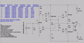
Here's my attempt at a schematic. The input device and VAS are the only suitable models I have; not too sure about voltage ratings.
However, I have adjusted input offset to achieve zero output offset, and set the quiescent to 125mA. You could go higher, of course. I have used a simple resistor to achieve this, rather than a Vbe multiplier.
I've added base stoppers, and used the 33pF lag comp you suggested.
Performance is not wonderful because loop gain is not high, will examine this later. Most of the distortion, however, is H2 and H3, starting around -60dB using +20dB as a reference.
Cheers,
Hugh
Attachments
.
Performance is not wonderful because loop gain is not high
Hugh
On the JLH SCA amp replacing the equivalent of R2 & P1 in your cct, with a current source worked wonders for performance - both in spice and in reality - I used that arrangement for a few years.
not sure if it would work here . . . but might be worth a try
mike
Last edited:
I believe that the performance is vastly determined by the capacitance of the second stage fet.. hence my suggestion of keeping the Zetex fets with very low capacitance..and here with the limited voltage rails.. 10 mA for driving the output should be possible...Else resort to laterals...
The current could also be distributed through a current mirror..
The current could also be distributed through a current mirror..
Last edited:
Lineup, all,
Thank you for your schematics and comments. I really like this design. It's almost like a FET JLH....well, I guess not, but as simple anyway.
As I mentioned in an earlier post I was working on something very similar with a BJT based input, but had not been able to get the bias/dc offset stable. Now I know why. I worked my way through lineup's schematic and thought about it and now have a better understanding of how it works. My problem was that I had not yet added feedback which cause the output to go to the rail with minimal bias/offset adjustment.
Now that I have added feedback I have managed to get it simming nicely in simetrix with 1A of bias. I'm definitely going to build this one using lineup's single jfet front end.
As I only need 10-20W of power I'm going to make a class A version...possibly with laterals.
Going to sim over the next day or two and try a few different layouts and VAS ccs topologies. I think I would prefer a bjt ccs for the VAS, as my (limited) experience has shown that BJT CCS's are more stable. If there's a good reason not to got this route, please enlighten me.
Will post back with a final proposed design for your perusal then order some parts. Will also look into lateral price and availability to help come up with the final design.
I'm very excited about this design. I really think it has the potential to quench my amplifier thirst for a while.
Mike,
Yes, makes a lot of sense, since it raises the loop gain almost an order of magnitude. This could be done easily but lag compensation would need to increase to preserve stability.
However, more feedback, while it reduces THD, smoothes FR and lowers output Z does create a longer spread of artefacts.
This circuit looks to have a loop gain of around 67dB, computed by examining the ratio of output to differential voltage across input and source of the input device.
I'm fairly sure small degeneration on the VAS would work well, but I'm limited in my models. You might note I've increased rail voltage for a bit more swing.
Cheers,
Hugh
Lineup,
Here's my attempt at a schematic. The input device and VAS are the only suitable models I have; not too sure about voltage ratings.
However, I have adjusted input offset to achieve zero output offset, and set the quiescent to 125mA. You could go higher, of course. I have used a simple resistor to achieve this, rather than a Vbe multiplier.
I've added base stoppers, and used the 33pF lag comp you suggested.
Performance is not wonderful because loop gain is not high, will examine this later. Most of the distortion, however, is H2 and H3, starting around -60dB using +20dB as a reference.
Cheers,
Hugh
Hugh,
Thanks for your schematic.
A few questions if you have the time:
1) What are the pros/cons of lineup's VBE/VGS multiplier versus the resistor you have used to set the bias? Also, what purpose does the parallel capacitor serve? Does using a fet based VGS multiplier provide better temperature stability?
2) What current are you running through your input jfet? I see you have used the same source resistor as lineup...does that value provide enough current for your chosen device?
3) Is the output zobel really required, especially if run in class A?
Your advice is appreciated!
Greg.
Hugh,
On my JHL I managed, even with the extra gain, with just about 30 - 50pF across the FB resistor - but I used some degeneration as well
In subsequent research on different designs I found splitting the compensation between FB resistor & gain transitor was an effective way of minimising the loss of OLG at high freqencies.
I guess this gives away that I'm true believer in the Church of High Feedback.
AKSA and othersLineup,
Here's my attempt at a schematic. The input device and VAS are the only suitable models I have; not too sure about voltage ratings.
However, I have adjusted input offset to achieve zero output offset, and set the quiescent to 125mA. You could go higher, of course. I have used a simple resistor to achieve this, rather than a Vbe multiplier.
I've added base stoppers, and used the 33pF lag comp you suggested.
Performance is not wonderful because loop gain is not high, will examine this later. Most of the distortion, however, is H2 and H3, starting around -60dB using +20dB as a reference.
Cheers,
Hugh
My models in SPICE shows some better behavior.
One thing I found, too, is the harmonics are mostly H2 followed by some H3.
My models for latest schematic below:
.SUBCKT ZVP3310A 3 4 5
* D G S
M1 13 20 5 5 Pmod1
RG 4 2 50
RIN 2 5 1E9
RL 3 5 1.2E8
RD 3 13 Rmod1 5
C1 2 5 55E-12
D1 3 5 Dmod1
D2 3 17 Dmod2
Egs1 2 17 2 5 1
Egt1 2 20 5 21 1
Vgt1 5 22 1
Igt1 5 21 1
Rgt 21 22 Rmod2 1
.MODEL Pmod1 PMOS VTO=-2.1 RS=2 IS=1E-15 KP=0.2
+CBD=35E-12 PB=1 LAMBDA=6E-3
.MODEL Dmod1 D IS=5E-12 RS=1
.MODEL Dmod2 D CJO=20e-12 IS=1e-30 N=10
.MODEL Rmod1 RES (TC1=9e-3 TC2=4.2E-5)
.MODEL Rmod2 RES (TC1=-2e-3 TC2=3e-6)
.ENDS ZVP3310A
.SUBCKT zvn3310a 3 4 5
* NODES: DRAIN GATE SOURCE
M1 3 2 5 5 MOD1
RG 4 2 356
RL 3 5 1E8
C1 2 5 21.5P
C2 3 2 2.5P
D1 5 3 DIODE1
*
.MODEL MOD1 NMOS VTO=1.736 RS=2.147 RD=1.682 IS=1E-15 KP=0.157
+CBD=25.5P PB=1
.MODEL DIODE1 D IS=6.12E-13 RS=.629
.ENDS zvn3310a
.SUBCKT MSK1058 1 2 3
* TERMINALS: 1 2 3
M1 9 7 8 8 DMOS L=1U W=1U
RD 1 9 80.4M
RS 3 8 5.28M
RG 2 7 21.4
CGS 7 8 410P
EGD 12 0 7 9 1
VFB 14 0 0
FFB 9 7 VFB 1
CGD 13 14 128P
R1 13 0 1
D1 12 13 DLIM
DDG 15 14 DCGD
R2 12 15 1
D2 15 0 DLIM
DSD 8 1 DSUB
LS 30 3 7.5N
LD 1 9 4N
.MODEL DMOS NMOS (LEVEL=3 THETA=85M VMAX=163K ETA=2.2M VTO=.2 KP=.999)
.MODEL DCGD D (CJO=128P VJ=.6 M=.68)
.MODEL DSUB D (IS=29N N=1.5 RS=61.4M BV=160 CJO=802P VJ=.8 M=.42 TT=252N)
.MODEL DLIM D (IS=100U)
.ENDS
.SUBCKT msj162 1 2 3
* TERMINALS: 1 2 3
M1 9 7 8 8 DMOS L=1U W=1U
RD 9 1 110.4M
RS 8 3 25.28M
RG 7 2 17.4
CGS 7 8 760P
EGD 12 0 1 2 1
VFB 14 0 0
FFB 9 7 VFB 1
CGD 13 14 467P
R1 13 0 1
D1 12 13 DLIM
DDG 15 14 DCGD
R2 12 15 1
D2 15 0 DLIM
DSD 9 8 DSUB
LS 8 3 7.5N
LD 1 9 4N
.MODEL DMOS PMOS (LEVEL=3 THETA=90M VMAX=183K ETA=6.5M VTO=-.2 KP=1.109)
.MODEL DCGD D (CJO=467P VJ=.6 M=.68)
.MODEL DSUB D (IS=29N N=1.5 RS=61.4M BV=160 CJO=900P VJ=.8 M=.42 TT=252N)
.MODEL DLIM D (IS=100U)
.ENDS
swordfishy
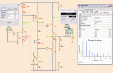
THis latest schematic below is for Class A and laterals 2SK1058/2SJ162.
Shows THD 0.006% at 20 Watt. (Max is about 25 Watt with +/-25V supplyy)
Note especially H2 harmonics dominant. At rather high level.
I recommend you use those transistors for lateral amplifier.
Zetex ZVN3310A TO-92
Zetex ZVP3310A TO-92
And run second VAS stage with those at 5mA
with only resistors to set bias.
The latest schematic
Attachments
My 2SK170BL model (8mA IDSS)
.MODEL 2sk170bl_8m NJF (AF=500.504m BETA=27.7612M CGD=19.8997p CGS=24p IS=10f
+ KF=.002229965f LAMBDA=1m RS=8.03465 VTO=-0.60)
Farnell has laterals for audio, dont remember the brand, maybe magnatec or whatever. Ok in price.. and i'm not talking about the buz devices now.
irf240/9240 if I remember correctly does'nt match very good. not in rds'on and not in transconductance. I believe I use irfp9140 and 240. not perfekt but better imho. And the gates has to be driven MUCH harder on hexfet, I think I use arund 50ohms or so.
studies have shown that hexfet as vas may produce a wider spectrum of crap than bipolars, if that is what one want's, fine. I would'nt go for that, plus ther is a considerable a omount of gate capacitance.
plus one have to consider what happens when it gets warm, even when it's in a low current use.
I always try the amps shorted with a 1uF and 100n capacitor to ground and with different loads and at different biases. It's completly possible with irf's too.
and come on now, it's not hard to get like 0.000000001% thd numbers in spice.
With all that said, yes if this path you're going down now is done correctly, it should sound very very good in the end..(it only took me 10+ years to get there).
MikelmHugh,
---
I guess this gives away that I'm true believer in the Church of High Feedback.
I am certainly one of that group, too.
But I do not like too many transistors. LIke to get as much gain as can be done with few transistors.
CCS constant current source is a friend of mine.
Did you download MultiSim 11?
As recommended by me in another topic.
This looks very nice. I like especially the feedback insertion (I'm a tube lover and it's mostly done like this way in tube amps). Although it is a pure voltage feedback in my opinion. The output voltage is divided and lies in series with input voltage (cause it is applied at the source of the jfet). Is there the possibility to apply the feedback at the gate of the jfet ? This would be parallel applied feedback (and this is the one I would call current feedback)
And another questiona bout the circuit in Post 29. If I want less Power cause of lower supply voltage, what do I have to change ? Only drain, source and feedback resistor of the jfet ? And if I use better mosfets (the zetex vor the driver and SEMELAB Laterals for the Power Amp) do I have to change anything in the bias topology ?
And another questiona bout the circuit in Post 29. If I want less Power cause of lower supply voltage, what do I have to change ? Only drain, source and feedback resistor of the jfet ? And if I use better mosfets (the zetex vor the driver and SEMELAB Laterals for the Power Amp) do I have to change anything in the bias topology ?
Lineup. What version of multisim are you using?
How did you import those models into multisim? Could you please discribe the process or give a link to the information you used to get the models to work in multisim?
I have had no problem with all the other spice programs I have used but importing models to multisim has got me beat... so far.
How did you import those models into multisim? Could you please discribe the process or give a link to the information you used to get the models to work in multisim?
I have had no problem with all the other spice programs I have used but importing models to multisim has got me beat... so far.
Me too, Mike, except I split the feedback..... nested and global.
Greg,
1. Very little sonically, except that Vbe multipliers tend to overcompensate bias creep with temperature on mosfet designs.
2. I'm using about 5.5mA, same as Lineup. The current through this device should be set however by R2/P1, rather than R4, so the jfet should be running well below Idss.
3. The output zobel ensures that the stage is loaded at very high frequencies, and it certainly provides additional stability for AB. In Class A, maybe no need, but frankly I'd want to build it and test it.
You can talk about these designs for eons, and people have, but it's a simple circuit, and while you can make educated guesses absolutely nothing beats building, measuring and listening to it!
Cheers,
Hugh
You can talk about these designs for eons, and people have, but it's a simple circuit, and while you can make educated guesses absolutely nothing beats building, measuring and listening to it!
Hugh,
Thanks for your answers. Good to know.
I have every intention of building it. Will order parts this weekend. Until then it seems silly not to optimise the design as much as possible with spice.
Lineup,
Would you mind simming the circuit with a J309 jfet front end and letting me know how it goes - if you have the model available and time to do it? This is the jfet I would like to use as it is easy to come by. You will need a much larger source resistor though.
If the J309 is no good, any through hole product that can be ordered from the fairchild website will do.
I have a model for the j309, but unfortunately not for the lateral output fets. Using vertical fets I have been unable to match your simulated figures, though they are still quite good.
Appreciate your help!
Greg.
- Status
- This old topic is closed. If you want to reopen this topic, contact a moderator using the "Report Post" button.
- Home
- Amplifiers
- Solid State
- JFET input, MOSFET VAS, LATERAL output = Perfect!!