No. This circuit uses a trick to overcome that limtation (hence the <1ppm dist. figure).A "Current Dumping White Follower" - CDWF, not bad !
Without any further in-detail inspection this device seems only to be very linear as long as its bias/idle current into the load is not exceeded, right ?
In this case, the idle current is less than 50mA, and in the sim, it operates at up to 2.5A^.
Q4 is part of the current mirror supplying Q7 a scaled version of Q5's collector current.
Im 100% sure, what I said.
Q3 is essentially held at constant current, up to the point, where more than -Ibias have to be supplied to the load, then it rises.
This means a rise of output impedance outside this crossover point and thus lots of distortion.
For this reason the amplifier works nicely at bias currents above 4A ...
I think my guessing is more accurate than your simulation !
Sims may have shortcomings, but they do have a decisive advantage: they have no preconceptions about how a circuit is going to behave.Im 100% sure, what I said.
Q3 is essentially held at constant current, up to the point, where more than -Ibias have to be supplied to the load, then it rises.
This means a rise of output impedance outside this crossover point and thus lots of distortion.
For this reason the amplifier works nicely at bias currents above 4A ...
I think my guessing is more accurate than your simulation !
Anyway, I'm in the process of perfecting the last details in the ultimate simulation: the one that uses solder, bolts, heatsinks, and similar components.
I am not too anxious about the result: I have already physically tested the most critical and contentious part of the circuit elsewhere, and it works as expected.
Here, it is combined with a Taylor follower, but I don't think the end result will differ much from the sim (which, BTW is what I expected).
Most time switching on your brains helps before doing a simulation, especially if you use a simulator, which is intended for SMPS simulations and you try to judge your amplifiers by THD1k at 10V.
And also: what is immediately obvious for some people, might be a preoccupation in the view of other people, but it nevertheless could be true ...
Did you try a DC sweep (-10..+10V) on V1 and look at the difference between input and output ?
Did you have a look at the difference between input and output with a 10Vp 20kHz sine ?
This should be a very ugly waveform with some neat spikes of switching distortion in it ...
This circuit is certainly not better than 0.01% THD20k in real life, perhaps 0.005%, if you use better semiconductors and a very very careful layout.
But you can prove the opposite, if you have a prototype running soon ...
congratulations!
This unity-gain follower is an audiological UFO/QUOTE]
did you built it?
and know the sound?
One advantage of Taylor, CFPs, and current dumping in general, may not be immediately obvious:
Emitter that must be the "follower" can be held at constant current.
And thats quite different than simply throwing a CCS under an emitter.
Correct and the Stasis approach tries to keep even the voltage of this transistor constant to eliminate any Early- and Miller Effects.
Unfortunately this only works nicely as long as the transistor actually sees a current and this is not the case in the here presented circuit with more than -50mA.
A sliding bias scheme with cascodes would be a nice thing ...
For the offset: R11 could be adjusted, or R10 or a combination of both.
Compensating unity gain buffers is not so obvious as compensating a "Blameless Amp", because these designs allow topologies, where the VAS is not as obvious.
I would call Q5 the VAS of this amp, so a miller cap could work here. On the other hand side it's base is driven at very low impedance, which could mess up the open loop phase response. A resistor in the emitter could be helpful as well, since the output stage can be seen as a current feedback amp. On top of this one could then put a RC from the emitter to GND, in order to increse the amp's noise gain, but this could give some heavy frequency response peaking ...
Unfortunately uncompensated amplifiers give the best distortion performance (at least in simulation, in real life they oscillate).
It is now built.did you built it?
and know the sound?
So far, I didn't feed it an audio signal.
I've had some problems, one totally unrelated to the topology, a very unusual defect of one of the transistors and the other was a high frequency oscillation (several MHz).
I could trace the origin of this oscillation: it was caused by the wirewound 0.33 ohm emitter resistor.
I made a quick and dirty fix, a 100n ceramic in parallel. Probably not optimal but sufficient to go on with the tests.
I didn't go very deep in details, in particular I didn't make attempts to check the linearity as it will not be easy, but at first sight the behavior of the prototype seems identical to the sim.
There is no way to set the offset: if the circuit is properly implemented, the offsets, both static and dynamic will be inherently correct.how to set the offset?
In short, any offset is caused by a difference between the Vbe's of Q5 and Q7, and the purpose of the compensation circuit is precisely to equalize the current densities of these two transistors.
This is not a deliberate choice: it is made necessary because the B-E resistor R5 must have a low enough value.why larger current through Q4,5 instead Q1,3?
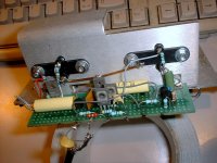
I didn't use heatsinks on the prototype, at 20V supply the TO126 becomes hot, but not excessively.do Q4,5 need the heatsink (~45mA idle through them)
In a working amplifier, heatsinks would be advisable.
The current version is for studying purpose, and some aspects are simplified or suboptimal.at higher supply voltage +-35VDC the oscillations at 20Vpp, how fix it?
Because Q5 and Q7 are of a different type and polarity, and are operated at different collector currents, some "curve fitting" is necessary to achieve a proper compensation.
This involves the divider R8/R9, plus an additional level shifting provided by R18.
The bias from R18 is OK at 20V, but at other voltages the compensation is upset, and as it relies on a controlled amount of positive feedback to work, this can cause oscillation (or under-compensation).
R15 also has an influence: it is necessary to make the circuit start reliably, but it also somewhat disturbs the compensation.
All these issues and some others will need to be dealt with properly in a real life usable circuit, but this prototype is a proof of concept and it has served his purpose.
Another peculiarity of this scheme is the input impedance: it not only non-linear, but also partly negative which can have disconcerting effects....
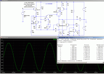
Here is a pic of the prototype, and the dynamic input/output offset with the collector currents of the output transistors:
Attachments
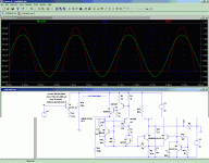
I carried out more detailed tests on my prototype.
The input-output offset has an amplitude similar to that of the sim, only slightly larger, but it has a flagrant even-order distortion.
I can reproduce an identical effect in the sim by entering the real value of R11, 0.22ohm instead of the 0.24 optimum, and by introducing a 1 milliohm resistor R16 in the output node, to take into account the non-zero resistance of the copper bus tying the various elements together.
All this leads to an undercompensation, sufficient to increase the THD by almost two orders of magnitude.
Those effects could be (and will be) rectified by a proper layout, and a more suitable value for R11.
Also, the real Q7 seems to have somewhat better characteristics than its sim model, and this contributes to the undercompensation.
One more thing that was expected, and is observed on the real circuit is that the topology demands a flat gain from the output transistors: the 2N3055's have a cut-off frequency of around 18KHz, and at this frequency, the circuit already begins to struggle to keep things under control.
Output transistors with an Ft of 5 to 10Mhz would be required to ensure proper margins.
Attachments
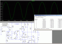
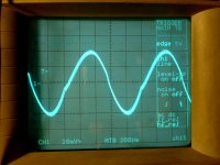
This is how looks of the input/output offset after some cleanup of the prototype.
The signal is amplified 20dB, the actual amplitude is 8mVpp.
The distortion of the residue is 7~8% and since the output amplitude is 20Vpp, this results in a THD of 30ppm.
(The waveform is unclean because the oscilloscope and distortion meter were floating, referenced to the output).
It is a far cry from the <1ppm of the sim, but getting close to these values would require a complete rebuild of the prototype.
I think that with some care, a figure of less than 10ppm is realistically achievable, without individual tweaking.
But even the 30ppm figure is not that bad: it is just an output stage in isolation, with no other NFB than that inherent in the CFP topology.
Attachments
I am watching with some interest... found this thread from another (of course).
My only comment is that if you need to add a "1 milliohm" resistor to anything to make it work right, the design is not "robust" enough for general application. There is more variation in even high precision parts than that... or in idiomatic english it's "too hairy".
_-_-bear
My only comment is that if you need to add a "1 milliohm" resistor to anything to make it work right, the design is not "robust" enough for general application. There is more variation in even high precision parts than that... or in idiomatic english it's "too hairy".
_-_-bear
Interesting design LV! Seems to me quite difficult to implement practically, so I am keen to see your final result. I've tried diamond buffers with reasonable success, but ended up going fo a simple follower inside an op-amp feedback loop. You can read the detials on my website.
Anyway, good luck with your project.
Anyway, good luck with your project.
If fact, you don't need to add a 1milliohm resistor: what is investigated is the effect of one parasitic milliohm at the wrong place.My only comment is that if you need to add a "1 milliohm" resistor to anything to make it work right, the design is not "robust" enough for general application. There is more variation in even high precision parts than that... or in idiomatic english it's "too hairy".
This might look "hairy" or over-sensitive or whatever you prefer, but you have to realize that achieving 1ppm with any topology requires a maniac attention to practical details.
For example, in a conventional amplifier, this would be equivalent to placing the global feedback take-off point some millimetres into the track to an OP transistor instead of the actual output node.
On a 4R load, you can roughly estimate that this would lead to a supplementary even order distortion of ~1/4000, that is 250ppm.
Did you say too hairy?
It works: I have built a proof of concept, and basically that's enough to satisfy me.Will this buffer idea fly or not??
_-_-bear
Maybe some day I'll include it in a complete amplifier, I'll just have to think of a matching VAS and input stage
The input stage would probably be a cross-quad variant, the VAS remains to be found.
- Status
- This old topic is closed. If you want to reopen this topic, contact a moderator using the "Report Post" button.
- Home
- Amplifiers
- Solid State
- UniGaBuf, a follower cut out to be a leader