You have to swap the "+" and "-" inputs of the op-amps. Right now you have a positive feedback.
Hi JensH
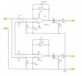
Thanks for your inputs but I still not sure how to swap the + and - inputs of the two op-amps therefore submitting a drawing will be highly appreciated.
nvm
thought about using transformers?
Hi qusp
Transformers are out of consideration for the time being. Thanks for suggestion.
Hi JensH
Thanks for your inputs but I still not sure how to swap the + and - inputs of the two op-amps therefore submitting a drawing will be highly appreciated.
Swap pins 2 and 3. Swap pins 5 and 6. That's all.
G²
Swap pins 2 and 3. Swap pins 5 and 6. That's all.
G²
Hi stratus
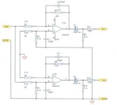
I have revised the schematic. Would you please check it for me?
Thanks
Attachments
Hi stratus
I have revised the schematic. Would you please check it for me?
Thanks
Looks like you nailed it. I think the junction of R2 and R4 should be tied to ground.
G²
Looks like you nailed it. I think the junction of R2 and R4 should be tied to ground.
G²
Hi stratus
You mean something like this:
Attachments
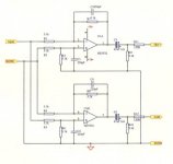
As long as you DO NOT connect the "SGND" to the output XLR's pin #1, that part is OK.
What about tying it 'loosely' with a low value resistor like 10-100 ohms? I've had very good success many times this way.
G²
As long as you DO NOT connect the "SGND" to the output XLR's pin #1, that part is OK.
Hi Kevin
Thank you for advice. It seems all the questions are cleared now.
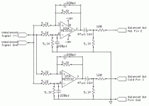
Since the top opamp inverts the input, its output should be labeled "Cold-" (and go to Pin 2 for US wiring of a balanced XLR connector) and the other one "Hot+" (and likewise to go Pin 3).Hi Andrew & Kevin
Thanks for the comments.
What do you think about this revision:
For even more on grounding and the "Pin 1 problem" there's the "White Papers" on this site - they're not ALL about selling audio isolation transformers:I should have also pointed out that the circuit's "SGND" buss may be connected to the chassis but probably not at the XLR connector.
WELCOME TO JENSEN TRANSFORMERS, INC.
Thanks for bringing this interesting topic up guys.
I'm having a debate with a friend about what the aforementioned sources (Rane, AES etc.) mean and your input would be appreciated.
From what I gather, the best way to do things is to ONLY have the chassis connected at pin1 and NOTHING else.
Signal and chassis ground should be tied together elsewhere, following a proper star grounding scheme (at the point between the filter capacitors for example), and not at pin1.
This friend of mine insists that using pin1 as the point where signal and chassis ground meet is a valid way to do things and does not violate the AES recommendations.
Your thoughts?
I just realized I made a mistake in my earlier post. It's too late to go back and edit it, so I've corrected it below in red - pin 2 should go to the "Hot" or positive-polarity signal:
Since the top opamp inverts the input, its output should be labeled "Cold-" (and go to [Pin 2] Pin 3 for US wiring of a balanced XLR connector) and the other one "Hot+" (and likewise to go [Pin 3] Pin 2).
As far as where to tie signal and chassis ground, I think it's a good idea to look beyond recommendations (not that they are wrong, they're not),and ask not just what works, but why.
The problem is (IMHO) most clearly spelled out in the diagrams on pages 9 and 12 of this document by Bill Whitlock:
http://www.jensen-transformers.com/an/generic%20seminar.pdf
The whole document is well worth reading, as it explains the safety reasons for various ground connections along power lines, within buildings, and within equipment. But in relation to hum, it's clear that any two devices powered by transformers connected to wall outlets will inevitably have an AC voltage between their chassis, regardless of whether either, both, or neither have the third prong "ground" connection at the power outlet. And when the chassis are connected, they will have an AC current flowing between them. The challenge is then how to connect them together so that this current does not generate a voltage that gets picked up in the audio chain.
This article describes a device to intentionally inject such current to test for immunity:
How to Test for the Pin-1 Problem, by Mary C. Gruszka
And here's the companion "fix it" article, but it doesn't say a lot that's applicable to this thread:
Resolving Pin-1 Problems, by Mary C. Gruszka
An unbalanced connection clearly does not do this (that is, it does not have full immunity to a current injected at the connector's ground), and it's remarkable that there aren't more hum problems between interconnected pieces of unbalanced audio equipment.
A balanced connection CAN do this, but there is still the problem that this current may go through (say) a PC board and across some small resistance of a copper trace which then generates a small voltage which then becomes injected into the audio. This is what makes the location of the connection critical. I see the goal as in tracing out the connection, see where the "pin 1 current" goes, and make sure any voltage drop along the way does not get into an unbalanced area of the audio signal path.
Connecting the signal (PCB) ground at the power supply to a common chassis ground seems to be a good way to do this. Leakage current from the transformer will go through this wire to the chassis which will then go to pin 1, but it will not go through the rest of the PCB.
Having pin 1 have hum in relation to the audio signals does NOT in itself add hum to the audio, as a proper balanced receiver circuit will not "see" the pin 1 voltage or current, but rather only the difference between the two balanced signals.
Perhaps the worst thing to do is connect pin 1 to ground at some point of the PCB, with the transformer secondary center-tap and chassis connected to another ground point on the PCB, where the pin 1 current will flow through the ground traces on the board.
I think this a possible cause of the problem, it seems natural to connect pin 1 to the same area of the PCB that pins 2 and 3 go, (that is, to the ground connection nearest the PCB connections for pins 2 and 3), but that is almost certainly NOT a good thing to do.
Just jumping in here so I apoligize if I am being redundant. Seems to be some ballanced line confusion. The idea behind balanced interconnects is you dont need a signal ground. The signal is transfered with no need for a reference to ground. In practice transformers do this the best. You can have large voltage differences in the grounds at the two ends of the interconnect and not affect your signal. In real balanced interconnects pin 3 is usually just for cable shield and connected only at one end (except for mics), signal is carried as a + and - voltage on pins 2 and 3 (and which is hot , only the manufacturer knows for sure) no ground needed or wanted.
Hi Everyone thank you very much for all your inputs. I still have the following question about this circuit:
What is the different between positive feedback and negative feedback of the unbalance to balance converter we have discussed in this thread? Since the original schmatic of this converter was illustrated with a positive feedback and we have revised it to negative feedback. Is the original schmatic a drawing error? Please advice.
What is the different between positive feedback and negative feedback of the unbalance to balance converter we have discussed in this thread? Since the original schmatic of this converter was illustrated with a positive feedback and we have revised it to negative feedback. Is the original schmatic a drawing error? Please advice.
Attachments

Hi Everyone thank you very much for all your inputs. I still have the following question about this circuit:
What is the different between positive feedback and negative feedback of the unbalance to balance converter we have discussed in this thread? Since the original schmatic of this converter was illustrated with a positive feedback and we have revised it to negative feedback. Is the original schmatic a drawing error? Please advice.
The first schematic will oscillate! + & - inputs are backwards.
- Status
- This old topic is closed. If you want to reopen this topic, contact a moderator using the "Report Post" button.
- Home
- Amplifiers
- Solid State
- Wiring a XLR plug