Hi,
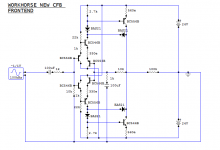
Most of the time CFB[current feedback] frontend has huge difference in input biasing current requirements. I came up with this new approach in order to balance the input current demand from both inverting and non-inverting nodes, so that it could be used like normal voltage feedback amplifiers. Bandwidth is spectacular and use of complementary rush cascodes at inverting side makes it very fast. Compensation networks are not used for simplicity, as its only a simulation yet. I don't know if similar topology exists or not, but its just i came up with...........")
Waiting for comments.
Kanwar
Most of the time CFB[current feedback] frontend has huge difference in input biasing current requirements. I came up with this new approach in order to balance the input current demand from both inverting and non-inverting nodes, so that it could be used like normal voltage feedback amplifiers. Bandwidth is spectacular and use of complementary rush cascodes at inverting side makes it very fast. Compensation networks are not used for simplicity, as its only a simulation yet. I don't know if similar topology exists or not, but its just i came up with...........
Waiting for comments.
Kanwar
Attachments
Last edited:
Member
Joined 2009
Paid Member
Wow ! looks very interesting indeed.
You will find a partner-in-crime with Keantoken:
http://www.diyaudio.com/forums/headphones/159815-rush-cascode-headphone-amp-jlh-output-stage.html
You will find a partner-in-crime with Keantoken:
http://www.diyaudio.com/forums/headphones/159815-rush-cascode-headphone-amp-jlh-output-stage.html
Thanks Bigun,
Keantoken is using single ended rush cascode only, whereas mine is fully symmetric design from input to output, an improvement in regular CFB frontend. I am thinking of making a mic preamp with this topology, because it permits the balanced input configuration with quite an ease like a normal opamp but with very high speed. There is still room for plenty of improvement like CCS in front EFs loading and so on.
Cheers
Kanwar
You add small hum supply on your signal path through 22K, using zener regulated will fine
I already stated that CCS are needed in frontend EF,s in my previous post. 22k is just for simplicity to check the operation of whole circuit.
Hi,
it looks like an LTP, but each half is a diamond arranged buffer.
Are the pairs of Qs attached to the 330e, the Rush Cascode?
Are the BAS21 diodes anti-saturation? or soft clipping?
Yeah both input nodes are diamond buffer arrangements.
Yeah the pair at inverting node followed by 330e are forming complementary Rush cascodes.
BAS21 diodes are for anti-saturation + non-sticky clipping.
It doesn't seem to be a CF amp; inverting input is high impedance. It looks like a revival of the 741 frontend...
Samuel
It is alternate version of typical CFB indeed, since the current is being fed to emitters only through the diamond buffer. The 741 frontend is totally different phenomena from this one. 741 suffers grossly in slewrate[0.5V/uS] domain, whereas simulation shows this circuit has slewrate in excess of 1000V/uS..........
Simulation shows this circuit has slew-rate in excess of 1000 V/us.
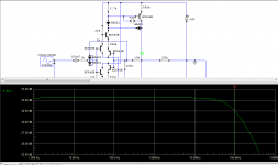
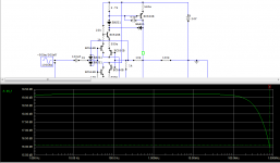
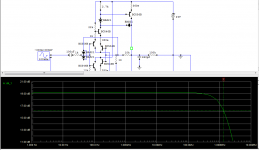
There are VF topologies which are free from first-order slew-rate limits and CF topologies which have first-order slew-rate limits. Hence slew-rate is not a (or at least not a sufficient) criterion to distinguish the two concepts. Key is if bandwidth is (as a first order approximation) independent from noise gain. How does frequency response looks like if you remove the 1k shunt resistor? And how when you set it to 100 Ohm? Also: what happens if you add sensible compensation capacitors, say 50 pF for each side--is the amp still as fast?
Samuel
Last edited:
There are VF topologies which are free from first-order slew-rate limits and CF topologies which have first-order slew-rate limits. Hence slew-rate is not a (or at least not a sufficient) criterion to distinguish the two concepts. Key is if bandwidth is (as a first order approximation) independent from noise gain. How does frequency response looks like if you remove the 1k shunt resistor? And how when you set it to 100 Ohm? Also: what happens if you add sensible compensation capacitors, say 50 pF for each side--is the amp still as fast?
Samuel
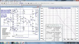
A pic speaks 1000 words,
You can see bandwidth with different compensations like miller Cdom[47pF on each complementary VAS collector to base] and Lag[from collector midpoint of VAS to GND] with both 100e and 1k in shunt.
Please note, I have simulated CDOM miller compensation just for illustration only, because in CFB topology miller compensation is not used. Though Lag compensation is used often to limit bandwidth according to application. With Lag compensation the Bandwidth is quite extended.
Kanwar
Attachments

Last edited:
In CFB topology miller compensation is not used.
Indeed traditionally CF topologies use one gain stage only (which must use shunt compensation), but this does not need to be so. There are many two-stage CF designs around, and all of them use Miller compensation. Just look up US patent 5537079; as shown on page 8 of the patent the two capacitors labeled CD are the Miller compensation capacitors, and they defined opamp bandwidth. Cp1 and Cp2 are just basically unwanted second-order capacitances which have no first-order influence on open loop gain.
The AD8011 (which is the amp described in the patent) would simply not work properly with shunt compensation. Your amp works with because the emitter resistors of the second stage are rather large, but I presume Miller compensation will give substantially lower distortion within the audio frequency range.
A pic speaks 1000 words.
Indeed. For both compensation schemes the amp has about 10x the bandwidth at ~20 dB than it has at ~40 dB (open-loop gain seems to be very low, that's why the actual figures are much lower than what the feedback network indicates). It is voltage feedback.
I hope you don't get my intentions wrong--I don't want to put your design down or anything. But to make the best out of it a proper understanding of its working principle is just a must...
Samuel
Indeed traditionally CF topologies use one gain stage only (which must use shunt compensation), but this does not need to be so. There are many two-stage CF designs around, and all of them use Miller compensation. Just look up US patent 5537079; as shown on page 8 of the patent the two capacitors labeled CD are the Miller compensation capacitors, and they defined opamp bandwidth. Cp1 and Cp2 are just basically unwanted second-order capacitances which have no first-order influence on open loop gain.
The AD8011 (which is the amp described in the patent) would simply not work properly with shunt compensation. Your amp works with because the emitter resistors of the second stage are rather large, but I presume Miller compensation will give substantially lower distortion within the audio frequency range.
Indeed. For both compensation schemes the amp has about 10x the bandwidth at ~20 dB than it has at ~40 dB (open-loop gain seems to be very low, that's why the actual figures are much lower than what the feedback network indicates). It is voltage feedback.
I hope you don't get my intentions wrong--I don't want to put your design down or anything. But to make the best out of it a proper understanding of its working principle is just a must...
Samuel
Hi,
I just glanced that patent and AD8011 datasheet, the input is simple differential with CFB as intermediate stage which ultimately drives the buffer, they are having CD as miller compensation no doubt about it.
Regarding my design, it does have a low open loop gain due to large emitter resistors , though i kept them intentionally low in order to keep the open loop response more linear, not heavily stressing upon global feedback to get required performance but one can tweak it to suit the different tastes. The open loop to close loop Gain variation at high frequency is more than regular CFB, but still its advantageous than classic differential input amplifiers we usually see in audio applications. If you compare it with normal LTP differential pair, it will still be having more bandwidth + slew rate. Since the classic LTP+VAS cdom compensation lacks in adequate slew rate which i have seen is limiting factor of the traditional topology, whereas this one is quite fast in that respect.
If you see the above plots you will find there is substantial difference in bandwidth in with miller and shunt compensation even with the same close loop gain. Shunt compensation works well in my design rather than miller.
Though learning is never ending constant process for me.
Kanwar
Last edited:
I came to similar result with a bit different approach, not rush cascode used but very similar result. http://www.diyaudio.com/forums/solid-state/253039-unique-cfa-120-230w-amp-16.html#post4428619
Attachments
- Status
- This old topic is closed. If you want to reopen this topic, contact a moderator using the "Report Post" button.
- Home
- Amplifiers
- Solid State
- My New CFB Frontend with balanced input biasing current requirements