")
Re: Changes to ClassAB-N-Ch
Hi!
Yeah! What semiconductors to use? Any special types in mind, or just rough specifications?
Bye
Arndt
Hi!
subwo1 said:Any suggestions or comments?
Yeah! What semiconductors to use? Any special types in mind, or just rough specifications?
Bye
Arndt
Hi.
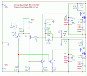
The BJTs are general "generic" types. The junction FET is given as a 2N5545, but you could use whatever you have and adjust the value of R3 to compensate for the different pinch-off voltge. The mosfets are IRF510, but the breakdown voltage is set higher than the rated 100V in the simulations I did.
The BJTs are general "generic" types. The junction FET is given as a 2N5545, but you could use whatever you have and adjust the value of R3 to compensate for the different pinch-off voltge. The mosfets are IRF510, but the breakdown voltage is set higher than the rated 100V in the simulations I did.
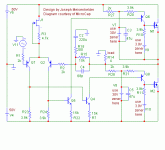
The first version probably has a dead zone (class C operation causing cross-over distortion). It looks like the quiescent current of the output stage in the second version is very dependent on the current gain of Q6 and Q8, as well as on the device parameters of M1, M2 and the JFET. At least you should add a bias adjustment potmeter somewhere, for example in the JFET tail current source. Try it with some form of current limited supply when you first switch it on, and see what happens if you use a hair dryer or so to change the temperature, because it is not clear to me how stable the quiescent current is going to be.
Q4,5,6,8 operating point.
Hi ,
I noticed that the Base currents of Q6 and Q8 are the collector currents of Q5 and Q4 respectively.
Is this your design point ? I would have expected the base currents to be much lower than the operating collector current in Q5 or Q4. Unless Ic of Q6 and Q8 is quite high and they have a low hfe.
Or maybe I have not understood the circuit well enough.
Cheers.
MarcelvdG said:The first version probably has a dead zone (class C operation causing cross-over distortion). It looks like the quiescent current of the output stage in the second version is very dependent on the current gain of Q6 and Q8, as well as on the device parameters of M1, M2 and the JFET. At least you should add a bias adjustment potmeter somewhere, for example in the JFET tail current source. Try it with some form of current limited supply when you first switch it on, and see what happens if you use a hair dryer or so to change the temperature, because it is not clear to me how stable the quiescent current is going to be.
Yes, the first version can be forgotten about. Your idea about the potential drift of the quiescent current is good; R3 could be lowered a little and a potentiometer placed in series with it. That would make the adjustment easier.
Re: Q4,5,6,8 operating point.
Hi.
The base currents of Q6 and Q8 can be allowed to decay without pull down resistors because they drive the MOSFETs, which have much higher input capacitance than the output capacitance of Q6 and Q8. The MOSFETs are allowed to operate fairly slowly, so I wasn't concerned about speed for Q6, and Q8. I hope I explained it well enough.
ashok said:Hi ,
I noticed that the Base currents of Q6 and Q8 are the collector currents of Q5 and Q4 respectively.
Is this your design point ? I would have expected the base currents to be much lower than the operating collector current in Q5 or Q4. Unless Ic of Q6 and Q8 is quite high and they have a low hfe.
Or maybe I have not understood the circuit well enough.
Cheers.
Hi.
The base currents of Q6 and Q8 can be allowed to decay without pull down resistors because they drive the MOSFETs, which have much higher input capacitance than the output capacitance of Q6 and Q8. The MOSFETs are allowed to operate fairly slowly, so I wasn't concerned about speed for Q6, and Q8. I hope I explained it well enough.
Yes indeed. IMO although this circuit works in the refined environment of a simulator it will not work in practice. Driving the bases of Q6 and Q8 directly from the collectors will cause a thermal drift problem (because the betas of Q6, Q8 will vary with temperature) and Q4 and Q5 will operate in a rather non-linear gain region as their Ic will be in uA. If you can make your simulator vary the betas you'll see the effect. In practice the betas will rise with temperature and the FET bias current will probably rise until they destroy themselves. Even if this works you'll have a distorted an asymetrical open loop gain.ashok wrote:I noticed that the Base currents of Q6 and Q8 are the collector currents of Q5 and Q4 respectively.
Ignore the simulator for a moment and try to work out the open loop gain through both FETs on paper. Consider what transistor parameters might vary and design your circuit to control them as necessary.
Re: Q4,5,6,8 operating point.
The main thing I like about the design is the way the mosfet gate drives are referenced to the sources. Having no base pull-down resistors on Q6 & Q8 made the idle current in the outputs easier to establish and increased the gain of Q5 and Q4.
But for now at least, I went ahead and added 1k pull down resistors to the bases of Q6 and Q8. I lowered R7 and R22 to 200 ohms each and for now, at least, shorted them together. Sharing the emitter currents may lessen cross-conduction and hopefully not produce crossover distortion while increasing the voltage gain of Q6 and Q8. The simulator at least did not show these changes as destabilizing the circuit as I had feared. These changes raised the idle current through R7 and R22 to 600mA each. .
.
The zeners hold down the gate drive power supplies so that the gates will not be damaged when Q6 and Q8 are fully on. The gates cannot go over 15V with the collector and emitter resistors having the same value as each other, and the gain of Q6 and Q8 is held to 1.
I think it is an interesing type of output stage. It appears to be fully symmetrical.
Umm, may have to try to compensate for the beta rise with temperature with diodes, especially one in the LED, bipolar junction transistor, resistors method as a replacement for J1. Alternately, I could go with the voltage regulated tail resistor. I like to start with a circuit with minimal parts and add more as needed. Also, the simulator is the demo version and doesn't simulate more than 50 parts, pretty decent, though. But I did try some changes around J1, Q6, and Q8.
Concerning the second diagram, I think the first stage has a gain of around 1 since there is a two volt drop across R3, the voltage amp stage has several decades worth, the mosfet driver stage would be around 1, and since the mosfets have a channel resistance of around 0.15 ohms, that stage would be around 30 with a 4 ohm load. I have tried some degeneration on the mosfets but gave up on that for now.
ashok said:Hi ,
I noticed that the Base currents of Q6 and Q8 are the collector currents of Q5 and Q4 respectively.
Is this your design point ? I would have expected the base currents to be much lower than the operating collector current in Q5 or Q4. Unless Ic of Q6 and Q8 is quite high and they have a low hfe.
Or maybe I have not understood the circuit well enough.
Cheers.
The main thing I like about the design is the way the mosfet gate drives are referenced to the sources. Having no base pull-down resistors on Q6 & Q8 made the idle current in the outputs easier to establish and increased the gain of Q5 and Q4.
But for now at least, I went ahead and added 1k pull down resistors to the bases of Q6 and Q8. I lowered R7 and R22 to 200 ohms each and for now, at least, shorted them together. Sharing the emitter currents may lessen cross-conduction and hopefully not produce crossover distortion while increasing the voltage gain of Q6 and Q8. The simulator at least did not show these changes as destabilizing the circuit as I had feared. These changes raised the idle current through R7 and R22 to 600mA each. .
.
millwood said:I like the bootstraping of the drivers (not sure if I understand why the zeners are used - can it be done without?).
I was thinking about a similar output stage (without the bootstraping) driven by a traditional VAS/input stage.
The zeners hold down the gate drive power supplies so that the gates will not be damaged when Q6 and Q8 are fully on. The gates cannot go over 15V with the collector and emitter resistors having the same value as each other, and the gain of Q6 and Q8 is held to 1.
I think it is an interesing type of output stage. It appears to be fully symmetrical.
traderbam said:
Yes indeed. IMO although this circuit works in the refined environment of a simulator it will not work in practice. Driving the bases of Q6 and Q8 directly from the collectors will cause a thermal drift problem (because the betas of Q6, Q8 will vary with temperature) and Q4 and Q5 will operate in a rather non-linear gain region as their Ic will be in uA. If you can make your simulator vary the betas you'll see the effect. In practice the betas will rise with temperature and the FET bias current will probably rise until they destroy themselves. Even if this works you'll have a distorted an asymetrical open loop gain.
Ignore the simulator for a moment and try to work out the open loop gain through both FETs on paper. Consider what transistor parameters might vary and design your circuit to control them as necessary.
Umm, may have to try to compensate for the beta rise with temperature with diodes, especially one in the LED, bipolar junction transistor, resistors method as a replacement for J1. Alternately, I could go with the voltage regulated tail resistor. I like to start with a circuit with minimal parts and add more as needed. Also, the simulator is the demo version and doesn't simulate more than 50 parts, pretty decent, though. But I did try some changes around J1, Q6, and Q8.
Concerning the second diagram, I think the first stage has a gain of around 1 since there is a two volt drop across R3, the voltage amp stage has several decades worth, the mosfet driver stage would be around 1, and since the mosfets have a channel resistance of around 0.15 ohms, that stage would be around 30 with a 4 ohm load. I have tried some degeneration on the mosfets but gave up on that for now.
- Status
- This old topic is closed. If you want to reopen this topic, contact a moderator using the "Report Post" button.
- Home
- Amplifiers
- Solid State
- Class AB