LED's are not noisy
Hi Sonnya,
Two people communicating in a foreign language can easely give rise to a misunderstanding.
So you do mean lowering the noise of the LED's. But I think the LED's are <B>not</B> noisy at all!. It is a different mechanism than in the zener or avalanche diode that are very noisy especially the above 5V types. In a moving coil cartridge preamplifier I once used a 3.3V zener. It was extremely noisy and uneven. You could hear the avalanche. Later I replaced it with a string of LED's. The noise was gone!.[Circuit is in fig. 7 of the MAT04 datasheet; low noise instrumentation amplifier]
Bases of the transistors of the current sources can by bypassed with a cap to ground, just to be on the sure side.
Please see the book Motchenbacher and Fitchen, Low-Noise Electronic Design, Wiley & Sons, page 180.
Hi again!
It is still worth trying even if the LED has LOW noiselevel. The LED bias resistor will add some noise to if it is bigger than ~ 1KOhm. Even if the LED has a low impedance, the transistor will generate some currentnoise on its base .... i think??
mmmhhh ... Elso .... figure 7 in the mat04 datasheet!?... try upload a new one ... haha
Sonny
Example of noisy zener in "low noise" circuit
Hi sonnya,
I am sorry it is fig.<B>6</B> of the MAT04 datasheet. I always look at the bottom of the fgure. I just downloaded the datasheet. Actually in the fig.6 it is a 3.9V zener(1N748A) but in the text the 3.3 V is mentioned because of the "soft knee". I have been using this circuit for a <I><B>balanced</B></I> moving coil cartridge preamplifier. Sounds very good. Hope this helps.
Mmmhhh .. Elso i have just read the thread through again. I will make a new design where i will make new currentsources. Make a new folded cascode, where i will enhance it with dual cascode.
The output stage - I think i will leave it as it is.
The JFET Q1 and Q2 ... I am going do make the layout so that i can interchange it with a Mat02 (Has a realy low offset .. 100 times better than the JFET's and a "linear" HFE)
I am going to make it as a doublesided PCB (5 boards 100*160mm can be done for ~2500DKR by ELPRINT)
I am going to use it for the MAT04 for the currentmirror .... if i can get them.
Sonny
I give up!
Hi sonnya,
I give up. Please have a look at this thread at the AudioAsylum!
http://www.audioasylum.com/audio/tweaks/messages/50592.html
Hi sonnya,
I give up. Please have a look at this thread at the AudioAsylum!
http://www.audioasylum.com/audio/tweaks/messages/50592.html
I don't want to fight with you!... LED's do generate noise .. take it leave it . It is still a PN design. It is right it does not generate a lot of voltagenoise.
Its series resistance applies to the diodeformula : ~ re = 25mV/A (at room temperature).
At a current of 100uA it will generate : ~2nV/sqroot(Hz)
At a current of 1mA it will generate : ~0.6nV/sqroot(Hz)
At a current of 10mA it will generate : ~0.2nV/sqroot(Hz)
Yes it is VERY small values .. Every time you raise the current your currentnoise will go up and it will multiply it self with the series resistor .. Wich also generate thermal related noise ...
I dont know the value of the currentnoise.. I have not been able to find any noisefigures on LED's at all!! It is not the normal application for LED's
The biggest reason i can think of why use a LED as refence is that it have the same Tempco as a transistor and to keep the circuit simple.
JFET do have noise figure around 3nV (For the J113). If you look at the currentnoise it is a lot lower than a BJT .. maybe 100times!
So you only end up with the 3nV and the thermal noise generated by the resistors and caps! surrounding the JFet.
If you choose the right JFET (in my case J113) to a specifiet current you end up with a ZERO tempco. Even if it would change 3% i would be happy .. The LED - transistor circuit can not do this much better... They say 2% over a complete temp. range
The reason why i was talking about to be able to interchange JFET Q1 and Q2 was to make hearing test on those . I wan't quit using JFET'S as a inputstage.. I was not happy with variation in IDSS!!!
You will have the same problem with DUAL's from unit to unit ...
I have not read the audioasylum link yet! I am going to do this know.
Sonny
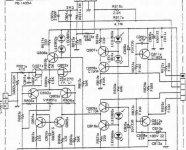
Luxman L410 schematic
Hi folks,
finally, I got the schematic from my friend and scanned the interesting part. It is the line stage, which works together in one part with the power output, so the biasing and the power transistors are missing.
BTW, the light emitting diodes are shown the wrong way round, the JFET is a N-JFET, and all transistors not marked differently are 2SC2320 or 2SA999. The minus voltage is top, the plus voltage bottom.
regards,
Hartmut from Munich
Attachments
What's up?
What do you mean exactly mikek?mikek said:folks...looks like Elso Kwak has got a something up his whatsit....
Read my first page......
sonnya said:First the schematic...
Match Q1 and Q2 (J111 - J113) to a current difference of 100uA when measuring IDSS.
Change R1 and R2 to 470R.
Change R3, R4, R14 and R15 to ~ 200R
Change R10 and R13 to 500R (multiturn)
Change R18 to 2K0
Set ID on Q3 to 6 - 8 mA.
Set ID on Q6 to ~ 6 mA.
Set ID on Q2 o ~ 2 mA.
Then it should idle around 30 - 35 mA.
The feedback is outside the PCB. Remember short tracks!.
Slewrate is ~+/- 75V/usec.
at unitygain -3dB is ~4MHz.
It is stable with 1nF load (No overshoot! at squarewave signal).
Try it!, i have mounted it inside my CD player and it have in my system better treble perfomance than OP275GP when driving
1K || 220pF load.
Sonny
Post #19, broken link to ED article(s)
This link and the other 'Walt's Tools and Tips' columns are apparently gone into the ether, from an ED website purge.
I have posted the 4 part ED op amp series on my website page under "Links, PDFs". This includes the discrete buffer referenced above with an LED Isource.
See: http://home.comcast.net/~walt-jung/wsb/
Enjoy.
wj
Hi Sonnya, Thanks for the links; two were new to me! Please find also below a link to a article by Walt Jung. He uses a similar buffer you do but with LED's in the current sources! GaAsP is just chemical shorthand for the chemical elements of gallium, arsenic and phosphorus used in the semiconductor. It looks very scientific but it is just a normal red LED [I am a chemist BTW] http://www.planetee.com/planetee/se...?ArticleID=2800
This link and the other 'Walt's Tools and Tips' columns are apparently gone into the ether, from an ED website purge.
I have posted the 4 part ED op amp series on my website page under "Links, PDFs". This includes the discrete buffer referenced above with an LED Isource.
See: http://home.comcast.net/~walt-jung/wsb/
Enjoy.
wj
Walt, your articles _can_ be found but I don't know the logic  beacuse they can't be found through search.
http://www.elecdesign.com/Globals/PlanetEE/Content/2800.html
I have now tried and tried. Why aren't "walt Jung" any good as search words? I have tried other words too without success.
beacuse they can't be found through search.http://www.elecdesign.com/Globals/PlanetEE/Content/2800.html
I have now tried and tried. Why aren't "walt Jung" any good as search words? I have tried other words too without success.
- Status
- This old topic is closed. If you want to reopen this topic, contact a moderator using the "Report Post" button.
- Home
- Amplifiers
- Solid State
- Jfet/bipolar PCB and Schematic (finaly)