peranders said:
The user interface isn't winning any rewards
I would recommend multisim Proffesional, Vs. 7, from:
www.electronicsworkbench.com
...state of the art, with highly intuitive user interface...
I've got some results of Hawksford cascode vs. Baxandall super pair for the VAS of the Lin topology. I'll just summarize what I got for the second and third harmonic for each configuration. Output signal was 20 kHz, 69.28 Volts peak, corresponding to 300 W into 8 Ohms.
Note that this is a low-feedback design, with very large emitter degeneration resistors in the diff amp (1k). Before you complain about the 1k resistors and tell me it's not a real world design, go look at the schematic of the LM3875 gainclone chip") .
.
I've posted the LTSpice files so you can duplicate the results if you're interested in doing so. They use a nifty TL431A behavioral model from analogspiceman of the Yahoo LTSpice user's group. This fixed all the convergence problems I was having with the TI-provided model.
Hawksford cascode:
2nd harmonic = -91.8 dBc
3rd harmonic = -106.2 dBc
Baxandall super pair
2nd harmonic = -90.2 dBc
3rd harmonic = -95.7 dBc
As you can see, the second harmonics are about the same with the two configurations. But the third harmonic is about 10 dB better with the Hawksford cascode. This is certainly much less of a gap than what I saw with the complementary design (20 dB difference for the third harmonic).
Based on this data, I'd conclude that the Hawksford cascode is a better solution - at least for this configuration of amplifier with +/- 90 V rails, 2N5401/5551 for small-signal devices and MJE340/350 for the final stage of the VAS.
Also, if anybody knows how to get rid of the phase inversion when clipping on the negative half-cycle of this design, I'd appreciate hearing about how to do it. I'm about ready to toss it into the trash bin in favor of the complementary design for this reason.
Note that this is a low-feedback design, with very large emitter degeneration resistors in the diff amp (1k). Before you complain about the 1k resistors and tell me it's not a real world design, go look at the schematic of the LM3875 gainclone chip
.I've posted the LTSpice files so you can duplicate the results if you're interested in doing so. They use a nifty TL431A behavioral model from analogspiceman of the Yahoo LTSpice user's group. This fixed all the convergence problems I was having with the TI-provided model.
Hawksford cascode:
2nd harmonic = -91.8 dBc
3rd harmonic = -106.2 dBc
Baxandall super pair
2nd harmonic = -90.2 dBc
3rd harmonic = -95.7 dBc
As you can see, the second harmonics are about the same with the two configurations. But the third harmonic is about 10 dB better with the Hawksford cascode. This is certainly much less of a gap than what I saw with the complementary design (20 dB difference for the third harmonic).
Based on this data, I'd conclude that the Hawksford cascode is a better solution - at least for this configuration of amplifier with +/- 90 V rails, 2N5401/5551 for small-signal devices and MJE340/350 for the final stage of the VAS.
Also, if anybody knows how to get rid of the phase inversion when clipping on the negative half-cycle of this design, I'd appreciate hearing about how to do it. I'm about ready to toss it into the trash bin in favor of the complementary design for this reason.
Attachments
Maybe emitter degeneration is the key?
Without emitter degeneration, the Hawksford cascode is just a regular cascode, because the emitter voltage becomes the same as the rail voltage.
While I have so far always used emitter degeneration in the VAS, I was considering not doing this in my next design.
The argument is essentially this: there is a certain amount of gain in the VAS stage, depending on collector current and collector impedance. Emitter degeneration is essentially local current feedback, so you give away some gain to have a more linear stage. As a consequence, there is less remaining gain so you need less Miller capacitance, and can still achieve roughly the same overall amplifier gain bandwidth and phase margin.
Without degeneration, all gain is available for feedback via the now bigger Miller cap.
- Overall VAS distortion should be roughly the same, the available"open" loop gain either being used up in the degeneration resistor and the small Miller cap or all in the big Miller cap.
- Overall GBW and lag should also be roughly the same
- The denerated version has the advantage (assuming this really is beneficial) of having a more constant gain through the audio band because its rolloff point is placed higher in frequency. However, there are probably ways to taylor the frequency response of the undegenerated VAS similarly.
- The degenerated version draws less current at high frequency thereby unbalancing the input pair less. The undegerated version probably needs a higher tail current to counter this.
- The undegenerated version has a much lower output impedance, which means its output voltage is much less influenced by nonlinear output stage input impedance. This might give you the same benefit that another class A follower stage would give you.
I wonder now what would simulate best (assuming compensation for identical GBW)
1) undegenerated, buffered (buffer between input pair and VAS)VAS
2) super pair without degeneration
3) super pair with degeneration
4) unbuffered undegenerated cascode
5) degenerated unbuffered cascode à la Hawksford
6) buffered undegenerated cascode
7) buffered degenerated Hawksford cascode
8)-14) everything with a post buffer between VAS and output stage
mikek said:
Hi Rickpt,
NE5534 is a good op amp....uses Johan Huising's nested miller compensation, together with a feedfoward path around the second stage...
...problem with the later, is that it generates a pole-zero doublets before unity-gain cross-over, which increases settling time.....
...this however, is unlikely to be of great significance in an audio power amp. with an output inductor fitted, as delayed settling resulting from normal ringing with said inductor is likely to swamp the effect of the doublet...
I agree with you but I think that compensation arrangement is the key for the excellent performance of the NE5534...
in theory it could be even bigger problem with a power stage...I’m planning to use a triple compound follower...
but I think it isn’t a big problem, music is much slower than test signals
this one will be a challenging project
Cheers
Ps: I don’t use inductor on the output stage...
rickpt said:
I agree with you but I think that compensation arrangement is the key for the excellent performance of the NE5534...
indeed this is true.....the NMC is responsible for its extraordinary linearity......it would probably be more linear if we could somehow do away with the feedfoward loop about the second stage....
This however this is a rather difficult preposition in a triple gain-stage design if good stability margins are to be maintained.
rickpt said:
...I’m planning to use a triple compound follower...
Good idea...of the Leach amp. variety....this is probably the best all round design around...in terms of closed-loop linearity...and freedom from annoying parasitic instability....
rickpt said:
Ps: I don’t use inductor on the output stage...
Not good...if you intend to inclose the output stage within the miller compensation loop.....
indeed this is true.....the NMC is responsible for its extraordinary linearity......it would probably be more linear if we could somehow do away with the feedfoward loop about the second stage.... This however this is a rather difficult preposition in a triple gain-stage design if good stability margins are to be maintained.
Maybe we could, at least I’m going to try, as the opamp has to be stable to lower closed loop gain, a thing that an amplifier doesn’t need...
Good idea...of the Leach amp. variety....this is probably the best all round design around...in terms of closed-loop linearity...and freedom from annoying parasitic instability....
I thought that the leach used a triple emitter follower...think of a normal compound follower with 2 transistor, but in the middle of the 2 transistors you have another emitter follower... maybe I will have some problems with this topology but I only will now when I build it...
I don’t care too much on stability margins if it's stable on my system, it's all a care, I don’t have to sell amplifiers
It's a known fact that overcompensated amps sound bad...
Not good...if you intend to inclose the output stage within the miller compensation loop.....
I plan to only test it, don’t think it will give satisfactory results regarding my previous experience with it,
thanks for your view on the project!
cheers
jcx said:The Super pair wins big as a VAS stage because it nearly equals the cascode on the output while increasing the input impedance, boosting the gain when driven with a current mirror. If you drive it from a collector resistor, I’m not surprised you didn’t see a big difference.
Simplest comparison I could come up with shows > 100x distortion improvement as a VAS over a single Q:
I suggest you use a buffered TIS, a la Self for a more meaningfull comparison......include the Miller cap....
super pair explained (sorta, maybe)
The 1st step in understanding the super pair is answering the question of how a CE stage with emitter degeneration can have MegOhm output Z when the transistor’s Zce may be as low as 20 - 50 Kohm. The incremental, heuristic argument is that the “extra”current flowing in Zce pulls up on the emitter resistor and Q emitter, reducing Vbe and cutting off the collector current in the transistor resulting in the emitter degeneration resistor’s current being held nearly constant. An equivalent small signal description is that the Zce current divides between the Q emitter and the resistor, the portion flowing in the Q emitter cancels most of the Zce current. The division ratio is the small signal resistance at the Q emitter to the degeneration resistance ratio: Re / ( 1/gm + Rs/hfe ) if Rs/hfe << 1/gm then the ratio ~= gm*Re and the net result is that the Zce component in the output current is reduced by this gain, or equivalently the Zce is multiplied by this gain.
In the super pair the input Q is current source biased and may be viewed as a common base amplifier, transferring the output transistor’s base current to the output Q emitter where the above current division-cancellation story is repeated for the small signal current flowing in the output Q base. The cancelled current includes the forward base current, essentially compensating for output Q hfe variation. The cancellation also applies to Zcb, particularly the “miller” capacitance term, which is important in limiting gain and linearity at high frequency.
This way of looking at the super pair also explains some of Andy’s disapointment with the super pair in his circuit, the MJE350 he uses as the output device has an hfe of ~18 @ 5 mA, limiting the gain available to correct the output Q error currents.
I’ve added another Q to the VAS in each of Andy’s example circuits, implementing some of Hawksford’s more intimidating looking composite super pair-cascode circuits to get around the low gain of the MJE devices in his circuit. I moved Ccomp and made it 2nd order to let more of the VAS gain be “visible” to the overall loop, the distortion results don’t vary much when a 68 pF C is added from VAS output to gnd to simulate the load of a simple miller comp Cap without hiding the gain of the VAS in a single pole miller integrator. The super pair with an internal cascode makes up some of the distance in the cmpnd_bax circuit @ -102 dB 2nd , but the “Hawksford” cascoded super pair in the cmpnd_hawk is still ahead @ -120 dB (with a little input stage linearization). At this point the 2-pole compensation is more to let the VAS stage potential be explored, it is definitely too twitchy for use with a practical power output stage with the present values.
(you still need AndyC’s zip for hi V Q models to sim these in SwCad)
Attachments
About the emitter resistor in your VAS configurations.
About the emitter resistor in your VAS configurations. Take the single transistor VAS with just a resistor.
I think the purpose of this emitter resistor is simply to ensure proper bias to the driving input current mirror.
Think about it : this transistor is current-driven, not voltage-driven. Because its base is fed from two collectors (the collector of a current mirror transistor and the collector of a diff pair transistor).
And these collectors will adjust their voltages so that the desired current flows in the VAS transistor.
"The incremental, heuristic argument is that the “extra”current flowing in Zce pulls up on the emitter resistor and Q emitter, reducing Vbe"
The knack is that Vbe does not matter really. It is just a side-effect of Ie as this transistor is current-driven. I agree Vbe varies, this would matter if the transistor was fed from a votage source, but not here.
I don't know if what I wrote is very clear...
Simulations I did show the collector impedance doesn't vary a lot when the emitter resistor is changed from 10 to 1000 Ohm.
IMHO this resistor is here to be sure the VAS base is a the right voltage so the current mirror feeding it doesn't saturate.
What do you think ? I'm not flaming you, if I'm wrong feel free to correct, but I just had to mention that.
A transistor is a voltage-controlled device; it’s just that the low impedance of the Vbe diode shunting the input requires a parasitic current when forward biased – defining Hfe, the current gain of the transistor, which is an important limiting parameter but not usually the defining “gain” in transistor circuits
The small signal gain is the incremental Vbe times the Gm of the transistor, the emitter resistor of the VAS reduces the effective Gm of the VAS and is a form of local negative feedback that increases input and collector-emitter impedances, bandwidth and linearity in proportion to the lost gain – with the high impedance drive from a current mirror, the increased VAS input impedance increases input voltage proportional to lost gain letting us get the improvements from local negative feedback in the VAS “for free” – because the voltage gain of the diff amp has been increased by the higher VAS input impedance
The feedback can be estimated as: 1+ delta_V(Remitter) / 26 mV and increases input impedance and the collector-emitter impedance, the total “collector impedance” includes the collector-base impedance which will dominate when the local feedback is high enough to increase collector-emitter impedance over the collector-base impedance value
I think Peufeu is appropriately treating the VAS transistor as a current in/current out device. In general I find it far more insightful to use the traditional beta model to try to understand what is going on. Mathematically, of course, it doesn't matter at all whether you first consider voltages or currents or transimpedances in the analysis. But remember that it is the electrons that are doing the work.
VAS Sims
Hello,
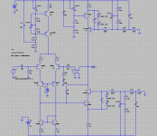
I just made a few simulations. Here is the circuit :
All the VAS stages ate fed a constant current from a constant impedance, which is the measured impedance of an input diff stage + current mirror, ie. about 70k.
These current sources are simulated by a constant voltage source in series with the source impedance (70k)
All the .define's below are here to calculate the right parameters for all the stages so they are all biased to 10mA no matter what emitter degeneration resistor we use. This works.
Thus we can study them open-loop. I took the problem in reverse order, put a voltage source on the collector and am varying collector voltage and looking at variations of VAS's Ic to calculate VAS collector impedance. As my collectors swing 1 VRMS, collector impedance is thus 1/delta Ic. Does everybody agree with that ?
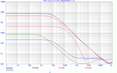
Now for the results.
Q3 (blue) = classic single transistor VAS
Q5 (black) = Hawksford Cascode
Q6 (purple) = Baxandall Super Pair
Q10 (red) = Normal Cascode
Q12 (green) = CFP
From what we see here, if highest colelctor impedance is desirable, Hawksford and the normal cascode look good, the others do not look so good...
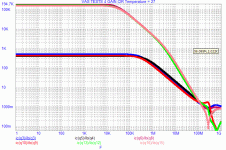
Hello,
I just made a few simulations. Here is the circuit :
An externally hosted image should be here but it was not working when we last tested it.
All the VAS stages ate fed a constant current from a constant impedance, which is the measured impedance of an input diff stage + current mirror, ie. about 70k.
These current sources are simulated by a constant voltage source in series with the source impedance (70k)
All the .define's below are here to calculate the right parameters for all the stages so they are all biased to 10mA no matter what emitter degeneration resistor we use. This works.
Thus we can study them open-loop. I took the problem in reverse order, put a voltage source on the collector and am varying collector voltage and looking at variations of VAS's Ic to calculate VAS collector impedance. As my collectors swing 1 VRMS, collector impedance is thus 1/delta Ic. Does everybody agree with that ?
Now for the results.
Q3 (blue) = classic single transistor VAS
Q5 (black) = Hawksford Cascode
Q6 (purple) = Baxandall Super Pair
Q10 (red) = Normal Cascode
Q12 (green) = CFP
From what we see here, if highest colelctor impedance is desirable, Hawksford and the normal cascode look good, the others do not look so good...
Attachments
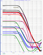
Interpretation
Yes, I pushed frequency to 1G even though it's rather meaningless, so we see better how the CFP wants to oscillate, for instance. These closely coupled transistors are touchy to get right.
On for the results. We are looking for the highest collector impedance, because this means less parasitic currents running through non-linear capacitances. A distortion analysis would be useful, but this AC analysis is a lot easier to do and gives a starting point for a better understanding of how these things work.
Black :
Hawksford cascode has the highest impedance, and it increases with Re (what's interesting is that the corner frequency does not look like it's moving). This is because this Hawksford Cascode needs a Re to work ! And the increase also depends on the source impedance : as the coupling cap transmits Ic variations as a voltage on the emitter of the lower transistor, the feedback will be stronger with a lower base resistor. Unfortunately we have a current source feeding this so high impedance can't be avoided.
Red :
Normal Cascode has the reverse effect : its imedance decreases as Re increases, but it still looks good.
Purple :
Baxandall Super Pair
This one really needs a Re to work. Looks like collector impedance is proportional to Re. With Re=1K it is as good as the normal cascode but its flat impedance goes higher. However the rolloff is sharper and there is a hint of instability.
Green :
CFP does not look good.
Blue :
Normal transistor
Re matters, so I guess I was saying ******** in my previous message. Sorry for that. However, even with Re, collector impedance is rather very low compared to the others.
So if the objective is to have a high collector impedance (hene high OL gain) to be able to linearize it with a Miller cap local feedback, these solutions look good :
- Hawksford
- Baxandall
- Normal Cascode
Hwoever, I did not take into account that the Baxandall has a higher current gain (two transistors = beta^2) which can also be very useful.
I will thus fire the underperformers and try some cascoded baxandall's.
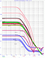
Ready to rumble
The new performers are :
Bright Green : Cascoded Baxandall
does not perform any better than normal Baxandall.
Pink : Hawksford + Baxandall
Gets into unbelievably high collector impedances. This is meaningless now, as PCB, air, and compensation cap leakage will probably swamp this (with what linearity ?).
Still, this is interesting. And what's more interesting is that it does not need a high Re to perform. And high Re are annoying, because voltage across Re is varying with the VAS current, introducing uncertainties in our perfect simulated world...
Attachments
Current Gain
Plotting the current gain (Ic/Ib) at constant collector voltage, we see the one-transistor VAS'es are all equal (beta = about 500) whereas the two-transistor VAS'es all stick to beta squared.
No surprises...
As it is very difficult to simulate the transimpedance as d(Vc)/d(Ib), we have to use our brains to relate these results to the prevous ones, and conclude that the Hawksford+Baxandall combo looks like the best (highest gain + highest impedance = highest overall transimpedance).
Attachments
- Status
- This old topic is closed. If you want to reopen this topic, contact a moderator using the "Report Post" button.
- Home
- Amplifiers
- Solid State
- Amplifier topology subjective effects