Sweet.
Building is on and now I just wait for some more parts to arrive.
I wonder, did anyone replace the 10K reesistors in the 82V-supply with zenerdiodes as indicated in one of the many schematics posted here?
Anyhow, a capacitorbank of 80 470uF will support the four 10000uF on the boards.
Two 625VA transformers on the way from Farnell. ending up like two monoblocks this one. Output transistors will be two three-pairs "stolen" from my TANDBERG-sparepart-storage. As mounting bracket for the heatsink there will be a custom made T-profile.
originally a 40X40mm, reduced to 40X30mm to fit the PCB.
Will fit perfectly since the 80 capasitors then will have perfectly space under the amplifier boards. Maximnum heat-transfer to the two sets of 385mm by 150mm heatsinks on each side. Transformers mounted near the front of the amp. Vertically on a steel bracket shielding them from the electronics.
I will post pictures as soon as there is anything to take pictures of.
Surely THE BEST AMPLIFIER I HAVE EVER HEARD can't be improved upon !!!!
I haven't heard it yet, as I am only in the starting phase of building it.
And I promise You: If anyone is capable of making this amp better, It's me.

And I promise You: If anyone is capable of making this amp better, It's me.
Sooner or later you end up with TANDBERG
Cool... Please show me the best Tandberg circuit I can build
But anyway, not everyone understand or will agree on the same concept of "better" amplifier. About everyone will end up with Tandberg, ehm, I haven't observed that phenomena. But I'm more than willing to build the best one proposed by you.
The signature is for fun purpose only.
Since TANDBERG is long gone, there is not possible for everyone to end up with TANDBERG. Too bad really.
Just name the class of power You want some schematics for, and I will provide what TANDBERG made in that area.
I could perhaps suggest their 220W amp? In 8 Ohms that is.
Nice one that.
Requires a HUGE cabinet, but actually well suited for the very advanced DIYer.
Last edited:
I have reexamined the schematics and simulation for this amp. I thought I understood it years ago but I only had a basic understanding. I didn't know what to think when Nagys kept saying it needs to be built exactly like the schematic. Now I realize there is plenty of truth to that.
This amp is designed for RF headroom (high slew rate) and phase linearity. I know this because the VAS and LTP are heavily degenerated. This allows compensation to be small, which loads the frontend less. The tradeoff is that DC gain of the frontend is very low, and audio band THD is increased. This may not be so bad, since the distortion is strongly H2 dominant due to the VAS Early effects.
This amp is pretty close to the edge WRT stability. Anyone designing a new PCB should know how to test for stability into capacitive loads. The transconductance of the FETs plays a major role in stability into capacitive loads, and so taking phase lead compensation from the output rather than the VAS could result in catastrophic instability depending on output loading, especially because of the very small L/R output network.
The output stage does not have good PSRR at RF; no output stage does. Because the LFET AC characteristics are important for the stability compensation of the amp, the rail response will be part of the output stage behavior and need to be exceedingly inert. I would not just slap films and large lytics onto the board else you risk oscillation. The 47uF decoupling lytics are important. I believe they provide damping for the rails. If a low-ESR lytic were used here it may cause instability. I would be interested to see the datasheet and ESR spec of the cap on the original Goldmund. For a given PCB layout, an appropriate RC snubber could be estimated for the rails that would hopefully dampen them well. I don't think it is enough to simply "pay attention" to decoupling of the output stage. One needs to measure and make sure the rails are inert or risk oscillation.
If this is done properly it seems to me that Goldmund could be unconditionally stable, as long as you leave on the output zobel. Of course it will ring into capacitive loads, but this is not a sign of instability, rather it's a sign of health because the amp is able to emulate a high-Q inductor. If this is a problem, the speaker cable should have its own customized snubber network, because while a stable amplifier's output inductance is either benign or with a lower limit, load reactance can vary widely.
Because the distortions of lateral FETs, FET input stages and this specific VAS are rather benign, the large RF headroom principle works well for this amp. I expect the next step if we wanted to improve the design would be to lower distortion while preserving the AC behavior.
I would not just slap films and large lytics onto the board else you risk oscillation. The 47uF decoupling lytics are important. I believe they provide damping for the rails. If a low-ESR lytic were used here it may cause instability. I would be interested to see the datasheet and ESR spec of the cap on the original Goldmund.
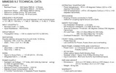
Here are the specifications on the Philips 47uF/100V capacitors used in the original MM9.2. They are of a long life type for industrial applications. Not a low ESR type.
Attachments
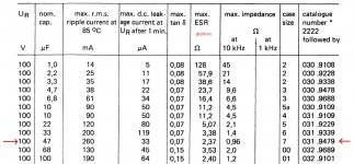
Thanks. That is like I thought.
In addition to a good ESR value, the damping cap needs to have a non-inductive path from the FET drains to output snubber ground. This may be difficult without a ground plane.
It seems whoever designed this amp either knew what they were doing, or made a very lucky guess. It would seem in some ways reliability was sacrificed for sonics, for instance with offset stability, and IIRC the drivers ran a bit hot?
Also, there is no need to turn around the protection zeners in the original schematic. They will still work this way. It seems they were oriented this way to reverse bias the 1N4148 to reduce the total capacitance of the limiter, and this makes sense for preserving the input impedance of the driver stage. I'm not sure whether the difference is really significant but it still functions as a protector AFAIK.
It seems whoever designed this amp either knew what they were doing, or made a very lucky guess. It would seem in some ways reliability was sacrificed for sonics, for instance with offset stability, and IIRC the drivers ran a bit hot?
At high output levels the VAS transistors runs at around 600 mW. The original MM9.2 design uses one clip-on heatsink for each VAS transistor, but the heatsinks are small. The driver transistors does not have this problem.
Hi tommy1000!
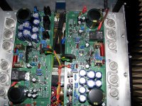
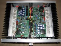
I also just completed amplifier similar to this amplifier, invite you to view images!
http://www.diyaudio.com/forums/solid-state/215127-637-amplifiers-10.html#post3322982
Thanks
I also just completed amplifier similar to this amplifier, invite you to view images!
http://www.diyaudio.com/forums/solid-state/215127-637-amplifiers-10.html#post3322982
Thanks
Sooner or later you will end up with GOLDMUND
I am about to. Soon.
Buying cabinet from Italy.
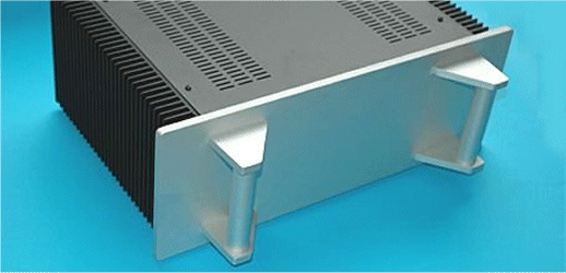
Without those handles, I think.
But they deliver every part of theese cabinets as spare parts.
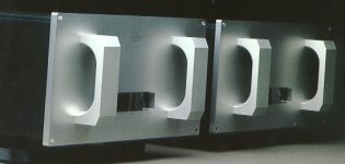
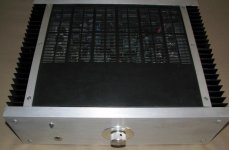
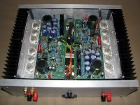
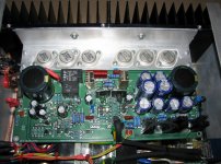
A teaser:
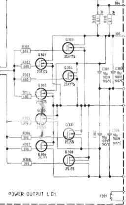
Are the lower devices shown inverted?
Not really, but I have seen this in many libraries, where they draw theese devices both this way, and with the gates the opposite way.
Nice having fun with theese .
At high output levels the VAS transistors runs at around 600 mW. The original MM9.2 design uses one clip-on heatsink for each VAS transistor, but the heatsinks are small. The driver transistors does not have this problem.
I also see it nessesary to add heatsinks for the VAS.
Theese will be made of some 1mm Coppersheet where I will make a transistor/copper sandwich of it all. Could ofcourse make some clips, and put on individually, bud the sandwich is so much easier to make.
My goodness what trouble one gets in.
Can anyone tell me where to get the 220uF 250V capaqcitors, with the quite narrow 16mm diameter there is left space for on the PCB?
Or better: What voltage do You guys have over theese capacitors?
I am building with 2X55VAC for supply, wich I have calculated to a voltage just over 155V over those. Can anyone confirm?
- Home
- Amplifiers
- Solid State
- The Very Best Amplifier I Have Ever Heard!!!!