Hi, i bought my boards last year (maybe 2) and i don´t know the right schematics em BOM, parts mask, etc...Now i want to populate them.
My boards (each one) have 6 Mosfets (TO-3) and was done by Nagys and Alex MM, the boards are revision 3.9. Somebody has the right schematics and parts lists ?
cheers
Hi HC, look page 224 for Liliya explanation
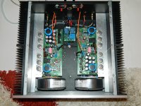
Looks like i got Nagys Amp with 2 pair transistor output
One thing i liked here, those PCB just need 40 VAC, so
i can use my transformer here 2x 0-45 vac hmmm all the
caps will be going to 80v or 100v
start with PCB, Transformer than start to look output
mosfet and other parts ...
start with PCB, Transformer than start to look output
mosfet and other parts ...
HCBONFIM has kindly sent his boards to me as a gift!!!

Hi smartx21,
By the way, did you received the boards yet?
According to mailing system website, it is quite close.
Hope to get them by the next week.
Thank you very much for this kindness.

I had a problem with Goldmund - Put the protection.
After much searching, I found that it shorted relay.
I did some measurements again and found some tension, which I do not know if they are OK ...
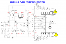
In pic Goldmund 1:
At T11:
B-1.2V
E-0.6V
At T12:
B-0.7V
E-0.18V
Bias - 100mA each final transistor.
(I did not put them 0.22R)
If you do circuit that pic Goldmund 2 - tensions are equal.
Noting that this problem is in both channels.
Audible sounds good but do not know if it is ok or I have a problem...
Thank you!
After much searching, I found that it shorted relay.
I did some measurements again and found some tension, which I do not know if they are OK ...
In pic Goldmund 1:
At T11:
B-1.2V
E-0.6V
At T12:
B-0.7V
E-0.18V
Bias - 100mA each final transistor.
(I did not put them 0.22R)
If you do circuit that pic Goldmund 2 - tensions are equal.
Noting that this problem is in both channels.
Audible sounds good but do not know if it is ok or I have a problem...
Thank you!
Attachments

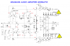
3mV of output offset combined with 2mV (76-74) of LTP differential seems to indicate that all is working correctly.
The voltages around the bss (T11&12) & output gates seem very wrong.
The PNP driver has a +ve voltage across the Vbe. It should be a -ve voltage for the PNP.
The voltages around the bss (T11&12) & output gates seem very wrong.
The PNP driver has a +ve voltage across the Vbe. It should be a -ve voltage for the PNP.

Sorry dear AndrewT , now it correct.
Gate voltages of P MOSFETS are wrong, double check it again, drain and source currents, and scope output, there may be oscillations.
Today I did all day measurements.
No signal input:
(B) T11 +1.2 V
(E) T11 +0.6 V
(B) T12 - 0.7V
(E) T12 - 0.28V
The oscilloscope can not see oscillations.
The input signal 1000 Hz voltages are almost equal :
(B) T11 +1.2 V
(E) T11 +0.6 V
(B) T12 - 1.1V
(E) T12 - 0.6V
Cleaned equality is preserved until the amplitude of 500mV.
If you grow stronger amplitude 550mV ... 800mV everything changes:
(B) T11 +0.35 V
(E) T11 +0.08 V
(B) T12 - 1.4V
(E) T12 - 0.7V
What I can not understand ... Although they are differences of tension during measurement 20Hz ... 100kHz sinusoid is perfect.
Last edited:
Today I did all day measurements.
No signal input:
(B) T11 +1.2 V
(E) T11 +0.6 V
(B) T12 - 0.7V
(E) T12 - 0.28V
The oscilloscope can not see oscillations.
The input signal 1000 Hz voltages are almost equal :
(B) T11 +1.2 V
(E) T11 +0.6 V
(B) T12 - 1.1V
(E) T12 - 0.6V
Cleaned equality is preserved until the amplitude of 500mV.
If you grow stronger amplitude 550mV ... 800mV everything changes:
(B) T11 +0.35 V
(E) T11 +0.08 V
(B) T12 - 1.4V
(E) T12 - 0.7V
What I can not understand ... Although they are differences of tension during measurement 20Hz ... 100kHz sinusoid is perfect.
Please check D3, zener 12V, D4, and T10.
Last edited:
Hello there ,
I installed Goldmund clone (from Big Panda) board which is upgraded to A2 according to NagysAudio instructions. When I test it feed +/- 50VDC and shorted input to GND, I cannot adjust R8 (R220) let the SPK output DC to zero. I right turn the trimmer to the end point still got 0.8VDC.
Out of this issue, all thing is well. Like the SPK AC meansure is about 0.6mV and the MOSFET tempature is OK.
So don't know how to handle this problem? Please share your idea , thanks.
"(E) T11 0.6 V (E) T12 - 0.28V" only 0.88v to open "BIASED" the two MOSFET final stage seems a little, I think your amplifier works in class B. Acording by datasheet SK134,SJ49 Gate-source cutoff voltace 1.45v u. need measured around T11 E+1.45V, T12 E -1.45V for running class A-B. thermal stability remain good questions,ideally u need R20 combination or replaced with super diode circuit, Mosfet output stage and equaly biassed around 50mA for all devices. good luck.
- Home
- Amplifiers
- Solid State
- The Very Best Amplifier I Have Ever Heard!!!!