oiphy:
''''T7-T8-T9-T10 - Thermal contact all four together!( I did exactly as proposed by Nikos on diyaudio)
Otherwise offset will not be stable!'''
TRUE
Also in my amplifier C7=4.7pf must fit to T7 not T8 for best results
and leave out the capacitor on T10. Μimesis 9.2
All these measurments with full load 8Ω
Hi.
so let's see if I got this right. C6 and C7 is taken away. then just linked.
C7=4.7pf must fit to T7 between B,C.
ok???
and in protection section D4 and D6 is 1n4148?
oh... some tips when firing it up???
thanks
Hello tony Ma, you are very welcome !
This is a project that NagysAudio started. I bought a PCB from him but the thread started a parallel project upgrading the original to a slightly superior version. You should read the complete story from scratch.
For many reasons the original version obtained less popularity and most of the examples and reports belong to de higher version ( 9.2 in place of 3 )
I left the project with all the components in a box for a long time and now I am trying to build it, but when I returned to the thread I had the problem of lack of information, some confusion about schematics, part numbering, etc.
You can see through the last posts that some experienced members have been helping me to put it all together. I am trying to have a complete picture and some of us here believe that the Goldmund Mimesis 3 clone is a very fine piece of equipment that gives outstanding sound results.
I have the original PCB, almost all of the BOM parts and I will try to follow the steps to get it up and running at my own risk. I know that some members have got excellent results from this first version.
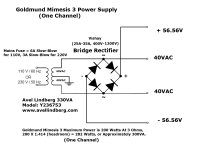
Please find the attached original circuit of the power supply and power transformer. If you go some posts back you will find lots of valuable information.
Roberto Berner
This is a project that NagysAudio started. I bought a PCB from him but the thread started a parallel project upgrading the original to a slightly superior version. You should read the complete story from scratch.
For many reasons the original version obtained less popularity and most of the examples and reports belong to de higher version ( 9.2 in place of 3 )
I left the project with all the components in a box for a long time and now I am trying to build it, but when I returned to the thread I had the problem of lack of information, some confusion about schematics, part numbering, etc.
You can see through the last posts that some experienced members have been helping me to put it all together. I am trying to have a complete picture and some of us here believe that the Goldmund Mimesis 3 clone is a very fine piece of equipment that gives outstanding sound results.
I have the original PCB, almost all of the BOM parts and I will try to follow the steps to get it up and running at my own risk. I know that some members have got excellent results from this first version.
Please find the attached original circuit of the power supply and power transformer. If you go some posts back you will find lots of valuable information.
Roberto Berner
Attachments
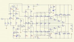
Dear friends, here is a first revision of my GM3 schematic.
Thank you oiphy, please check if Vitali's appreciated advice is well reflected here.
Protection circuit transistors are named Q1, Q2, etc. Protection components are numbered 101, 102, 103 ... etc because the original circuits overlapped numbering, so amplifier and protection components got confused.
Amplifier transistors are T1, T2, etc. and I tried to copy the same distribution as in GM 9.2 so we can understand all comments about GM 9.2 applied to GM 3.
Please feel free to catch any of my errors and report.
Thank you very much.
Roberto Berner
Attachments
Dear friends, here is a first revision of my GM3 schematic.
Thank you oiphy, please check if Vitali's appreciated advice is well reflected here.
Protection circuit transistors are named Q1, Q2, etc. Protection components are numbered 101, 102, 103 ... etc because the original circuits overlapped numbering, so amplifier and protection components got confused.
Amplifier transistors are T1, T2, etc. and I tried to copy the same distribution as in GM 9.2 so we can understand all comments about GM 9.2 applied to GM 3.
Please feel free to catch any of my errors and report.
Thank you very much.
Roberto Berner
Looks good to me
")
prot: maybe give the caps value in volts? remember some members may use trafos 2x55v....
C7=4,9pF could be moved to B-C T7 from T8.
OH the most important tingi... buildguide with plenty photos.
With this words I wish u good luck and happy building.
maybe making a bom?
stig
Last edited:
I am trying to understand this goldmund clone.
Can any one can direct me more detail?
Like transformer information, chassing etc
tks
Which one? there r several just in this thread. Can send you some on epost if you like.
Which one? there r several just in this thread. Can send you some on epost if you like.
Looking for the latest goldmund design with BOM
But i read some user name by Nagysaudio?? banned... and looked the site .... OMG the PCB cost 130 for DIY come on.....
that make me think about this project (I feel that DIY should not be so commercial)
tks
Last edited:
Hello
What is the purpose (function) of the BD249C BD250C transistors in the circuit. It may sound stupid my question but I never used transistors in any circuit such a way like that...
Can you explain in a small detail please..
The reason I ask because the Goldmund Tellos does not have all do that a famous Goldmun circuit to.
Thank you very much
Greetings Gabor
Attachments
Hello
What is the purpose (function) of the BD249C BD250C transistors in the circuit.
They form a floating separate power supply for the input, VAS and driver section of the amp. The telos 1000/2500 models uses separate full wave bridge rectifliers in this position instead.
The BD249/250 form regulators which are used to power the input and VAS stages of the amp. A voltage doubler followed by a regulator is used to provide a slightly higher voltage to the first stages, presumably to reduce noise and to allow the outputs to be driven closer to the rails.
protection part:
C1,C2 220uF volt rating? low esr?
C3 1uF volt rating?
thanks
The original design used 220uF/10V non low ESR and 1uF/63V. This may be to low voltage if the mosfets blows.
The original design used 220uF/10V non low ESR and 1uF/63V. This may be to low voltage if the mosfets blows.
thank you
thanks for your good jobDear friends, here is a first revision of my GM3 schematic.
Thank you oiphy, please check if Vitali's appreciated advice is well reflected here.
Protection circuit transistors are named Q1, Q2, etc. Protection components are numbered 101, 102, 103 ... etc because the original circuits overlapped numbering, so amplifier and protection components got confused.
Amplifier transistors are T1, T2, etc. and I tried to copy the same distribution as in GM 9.2 so we can understand all comments about GM 9.2 applied to GM 3.
Please feel free to catch any of my errors and report.
Thank you very much.
Roberto Berner
i like creat one
can i use this amp in my car?
is it stable for 2 ohm empedanse?
do you have pcb for that?
thanks friend
- Home
- Amplifiers
- Solid State
- The Very Best Amplifier I Have Ever Heard!!!!