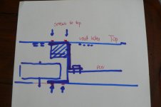
Here is what I will do. I rotate the board (thank Jaco!) I'll find or make C bracket to fit the Chassis top to bottom . I will attach L bracket to it as shown on the other side of C bracket . I'll either fit heatsinks from both sides of tranformer or square bar. I"ll attch the divider bracket to sides heat sinks top and bottom with plenty of heat sink compound . I'll make vent holes on the top bottom over transistor board. I will have transformer in separated compartment and plenty rigid chassis. I'll wait for transformers and than I'll get to it.
Attachments
Was there ever any artwork produced so that us true DIYers could produce our own PCBs? Trawling through the threads, there were several artwork designs that included the component overlays but I couldn't find a definitive one that everyone was content with and that didn't have anything other than the copper traces.
I've been INCREDIBLY impressed with my Pass Aleph 4, as others have compared even this leviathan with the BAIHEH, I thought it must be worth giving it a go.
I've been INCREDIBLY impressed with my Pass Aleph 4, as others have compared even this leviathan with the BAIHEH, I thought it must be worth giving it a go.
as shown on the other side of C bracket.
Same mistake, look at the road the heat will have to travel : thermal bottleneck.
Making the heat travel across a distance through the bracket to reach a much larger thermal inertia is a guarantee for temperature fluctuations.
Remember this is a Class AB amplifier.
The square bar has to hook up with the corner of the L/C bracket for unrestrained heat flow.
Make the cross-sectional area of the bar large enough, and heat travelling to the left and right for the heatsinks will not be such an issue.
Still a patch, ideal still is a heatsink straight at the output devices.
For completeness :
Lateral MOSFETs are different animals, compared to verticals.
Both are prone to oscillation due to parasitic capacitances and inductances, but Vertical MOSFETs are pussies in comparison to Laterals.
Positioning Vertical MOSFETs far apart in a Nelson Pass Class A power amp design is preferable, but Laterals in a Class AB should be as close together as possible, spreading them out wide apart on a heatsink is a No-No.
Any wire has inductance, the reactance that follows has a linear relationship with frequency : frequency up, reactance up.
With parallel devices, the inductance between the sources of two devices makes them influence eachother.
Placing MOSFETs farther apart means a longer connection between the sources of the devices, more inductance.
Lateral MOSFETs are more susceptible to reactance.
And what does the GM have ?
- Several parallel devices !
- Lateral MOSFETs !
- Frighen high bandwidth !
Last edited:
Jacco, my idea was to make an internal heatsink out of 4"x9.5" (lxh) C bracket. I will either do this or just bolt each board to one heatsink with an L bracket as intended and make new stereo chassis with two transformers in the middle. It will require the same amount of work and will cost only a little more to make front ,back ,top, bottom pannels. I will not have transistor board on wires , it's horrible for repairs troubleshooting etc.
Attachments
Last edited:
I wonder if somebody who has already build this amp could setup a website with all the information he has needed to build it. With used PCB, schematics and BOM and teaks.
Maybe we should setup a wiki page for this Goldmund project. Everyone who has experience with building it could contribute to this wiki. We could also gather links on the wiki website to people who are selling PCBs or other parts. Because meanwhile it is very hard to filter out the relevant information out of these 200 pages for a successful build.
I could setup a wikipage on my webserver, but I haven't build one yet and would need experienced people to contribute to this wiki.
What do you think?
Last edited:
Can I please re-iterate my previous question.
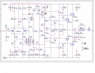
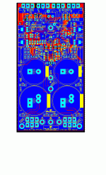
Was there ever a final PCB layout suitable for DIY etching ?
Was there ever a definitive BOM.
Was there ever a comprehensive schematic.
Sure, there aren't such final PCBs, BOMs, and a schematics in here.
But there are people who have successfully build such an amp. And if we take the PCBs what they took, ask them for their BOM and document maybe also their PSU they have used and so on, it's should be sufficient to get one work without reading thru these 200 pages of this thread.
That's why I ask for experienced builders and want to encourage them to share their experience. Maybe in an own website, in this forum or what ever. Otherwise all the 200 pages of discussions about optimizations of this amazing amp and how to do-it-yourself was for the birds...
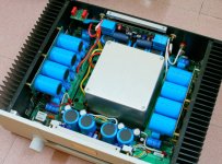
Here,Goldmund clone vesion low cost similar Metis 3 or 5
But that is NOTHING like any other post in this thread.
Attachments
Last edited:
Sure, there aren't such final PCBs, BOMs, and a schematics in here.
But there are people who have successfully build such an amp. And if we take the PCBs what they took, ask them for their BOM and document maybe also their PSU they have used and so on, it's should be sufficient to get one work without reading thru these 200 pages of this thread.
That's why I ask for experienced builders and want to encourage them to share their experience. Maybe in an own website, in this forum or what ever. Otherwise all the 200 pages of discussions about optimizations of this amazing amp and how to do-it-yourself was for the birds...
The information just isn't there. I have spent all afternoon reading the thread and the basics are just MISSING.
But that is NOTHING like any other post in this thread.
Yes,many peoples clone Goldmund amplifier => many versions.
I have got >3 versions.
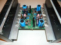
Two heatsink lelf and right.
Attachments
its in another thread lol .... should I tell you about it?
Yes please.
The information just isn't there. I have spent all afternoon reading the thread and the basics are just MISSING.
I'm not sure if this goldmund amp is the right DIY project for beginners. Or what do you mean with basics?
That PCB thread in #1954 is dead. There is another one that was started in the past month or two that may still be active. It's for a different Goldmund board.
See here: http://www.diyaudio.com/forums/group-buys/208429-gr-diy-telos-amplifier.html
See here: http://www.diyaudio.com/forums/group-buys/208429-gr-diy-telos-amplifier.html
This thread is not dead.
http://www.diyaudio.com/forums/group-buys/175296-pcb-order-goldmun-clone-33.html#post2764836
http://www.diyaudio.com/forums/group-buys/175296-pcb-order-goldmun-clone-33.html#post2764836
That thread is still open but not popular now. I still have some boards for them. If you are not serious, do not ask me to send invoice. Too many chicken-outs (after issuing invoice) .
4shared folder - goldmund
4shared folder - gm_white
4shared folder - goldmund
4shared folder - gm_white
But that is NOTHING like any other post in this thread.
I said very clearly - we did just after NagisAudio's original scheme.
Carefully read everything he wrote Nikos and understand how to get a good result.Bigpanda expect your order to PCB.
Nikos, once again - Thank you!
- Home
- Amplifiers
- Solid State
- The Very Best Amplifier I Have Ever Heard!!!!