Alex your boards always look nice. What software do you use?
If people are happy with a routed board I may be able to oblige if I can obtain the correct files. Please realise that in order to build these kind of boards you need to work to a paper printed or on-screen layout of components. An order for 4 pairs or more would be needed.
I sure would like to have some nice machine routed pcb's of this amp produced. Does anyone have any reservations to this.
Now how do we get the files to a job shop.
If people are happy with a routed board I may be able to oblige if I can obtain the correct files. Please realise that in order to build these kind of boards you need to work to a paper printed or on-screen layout of components. An order for 4 pairs or more would be needed.
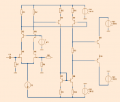
I haven't seen this kind of topology in other amplifiers, per se. Which amps are almost identical?
There are no amplifiers that are very close to this one. What I know.
What I meant was the basic Input-VAS topology.
If we boil it downto a very simplified circuit.
1. input diff pair
2. another pair with mirror at bottom for vas
I we replace input JFET pair with two BJT, (and remove cascode)
then we get close to the Input + VAS of NE5534, the wellknown Opamp.
See my diagram, as to what I think this amp is.
For example SymaSym uses a similar setup.
Sometimes R3 + R4 is put together to one resistor.
There are plenty of details that together makes this amplifier unique.
We have already mentioned the regulated input-vas supply.
Dont know what voltage, but caps are 100V, so I just put 90 Volt för input-vas.
We should also notice the very simple bias of output.
Just one resistor between the output drivers!
With those old laterals this was very common.
Because it worked. Will not work very well with HEXFET, like IRFP240
Attachments
Yes, the amp is stable at a 2 ohm load.
The only difficult parts to source are the 2N5565 dual metal can military jfets. They are expensive, but you can still find NOS ones on eBay, usually from the UK.
The Hitachi mosfets are also difficult to source, but the PCB layout has been updated with new easy to find Hitachi mosfets.
This is a very nice PCB board, it's tempting, so I would also be interested in purchasing one, if you guys do a group buy. But I would only want one if the PCB board is upgraded back to include the original 2N5565's and either 3 pairs of mosfets, or two pairs.
The Mosfets are too closely spaced. The individual mosfet decoupling capacitors shown on the original schematic have been omitted. Local decoupling is important to maintain stability, especially on a wide bandwidth amplifier.Does anyone have any reservations to this
The PCB layout shown seems to require 2 vertical heatsinks or a tunnel type heatsink per channel. This can get expensive and is problematical if fan cooling is is used as it would mean cooling the mosfets from one side of the pcb, which encouages a thermal gradient across the mosfets.
I would have thought that this amplifier could easily drive the mosfet pairs on a separate PCB. The Output stage can then be set out to allow for optimal cooling and decoupling. The overall cost of of the amplifier would be decreased.
If a single PCB layout is preferable the maybe the mosfets should be repositioned so that they are in a single row.
The output mosfets as they are positioned on Alex MM's PCB really would require the mosfets on the underside of the PCB and the copper on the topside, so that the mosfets can all be mounted on one flat face of a heatsink.
I did a quick parts search and these items are a little bit pricey. Though I guess there is not price tag for quality.
Avnet had the best prices on the outputs so far, quite a few thousand in stock. The Renasas site shows these items in current production so counterfeits should not be a problem.
We are going to have to have two separate frontend regulators and the output section power supply. A pcb for that would be REAL nice.
I can not think of any commercial company, too date, that has done this.
I want one. Tad
I see the decoupling capacitors in Alex's PCB. They are most definitely required as the amp could oscillate without them.
The mosfets could be spaced a little farther apart, but that's not critical.
Alex, I would remove the small heatsinks from the PCB. The BSS71/BSS74 don't need a heatsink. Can you move the BD249C/BD250C closer to the mosfets? They should be mounted right by them on the same heatsink.
The mosfets could be spaced a little farther apart, but that's not critical.
Alex, I would remove the small heatsinks from the PCB. The BSS71/BSS74 don't need a heatsink. Can you move the BD249C/BD250C closer to the mosfets? They should be mounted right by them on the same heatsink.
...dual jfets 2N5565's are obsolete and dificult to find, but they are significantly superior to 2SK170's. ...
Why do you think that 2N5565 is superior to 2sk170 (let alone "significantly") ?
There is no single parameter in datasheet that leads to that conclusion, and for the price of one 2N5565 you can buy a hundred of 2sk170 and find even better matched pair between them (not to mention even better and cheaper part, BF862).
Nelson Pass raves about these Semisouth power J-Fets; these seem to have less distortion than lateral mosfets. Maybe an option here?
My Yamaha B2 power amp has a front end with regulated power supply (+/- 80V), and power J-fets.
Japanese high-end technology of some thirty years ago.... but still sounding excellent.
Pieter
My Yamaha B2 power amp has a front end with regulated power supply (+/- 80V), and power J-fets.
Japanese high-end technology of some thirty years ago.... but still sounding excellent.
Pieter
Why do you think that 2N5565 is superior to 2sk170 (let alone "significantly") ?
There is no single parameter in datasheet that leads to that conclusion, and for the price of one 2N5565 you can buy a hundred of 2sk170 and find even better matched pair between them (not to mention even better and cheaper part, BF862).
Why is BF862 Superior?
Sidenote: Maybe a GB on the expensive components as well as pcbs would be worth a thought?
SemiSouth devices have no P-channel counter-part......Maybe an option here?...
Why is BF862 Superior?...
Higher transconductance, lower parasitic capacitance, lower noise...
They are better because both jfets are in the same metal can. The temperature for both jfets is extremely close. This is very important in an input stage. If you look at my original schematic, the OP input stage module can also be potted.
It's not important at all since it's ver easy to thermally couple the 2sk170 JFETs.
Actually, 2N5565 have more noise and lower transconductance. Also, the transfer characteristics are far more non-linear.
They seem to have disappeared in the 4 output pair PCB.I see the decoupling capacitors in Alex's PCB. They are most definitely required as the amp could oscillate without them.
Also current sharing resistors have been added to the source outputs. Would you just link these out?
Pioneer A70 from 80' is 'The Very Best Amplifier I Have Ever Heard'
Dual FET, Cascode, DC servo, Non Switching bias circuit, classG output...
Try to DIY it")
I'll do better than try... It's mostly done. My pioneer M-90 based "PX" is VERY close to that A-70 (thanx for that). I see a few more "tricks" in the A-70.
OS
I'll do better than try... It's mostly done. My pioneer M-90 based "PX" is VERY close to that A-70 (thanx for that). I see a few more "tricks" in the A-70.
OS
Also separated and regulated power suply for VAS... many diyers just ignore 'tricks' from commercial amplifiers, and say 'this is not audiophile amp', but diy amplifier based on this amps can be 'the very best', you are on right way,
Regards
Last edited:
Higher transconductance, lower parasitic capacitance, lower noise...
Seems like a good answer to me!
And for 24 cents no less!
- Home
- Amplifiers
- Solid State
- The Very Best Amplifier I Have Ever Heard!!!!