Hi
I have started an amplifier design and have found that LM4780 is a good choice. I examined datasheet and thought that reference PCB design is complex and big.
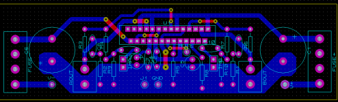
I have designed a smaller PCB, wherein i used LM4780 in inverting configuration. But i have doubts on grounding. Datasheet says that a star ground is good but instead i have placed a large ground plane and placed as much possible as ground connections on the plate.
Any opinions?
BTW, later on i may post .dsn .lyt (proteus) files.
I have started an amplifier design and have found that LM4780 is a good choice. I examined datasheet and thought that reference PCB design is complex and big.
I have designed a smaller PCB, wherein i used LM4780 in inverting configuration. But i have doubts on grounding. Datasheet says that a star ground is good but instead i have placed a large ground plane and placed as much possible as ground connections on the plate.
Any opinions?
BTW, later on i may post .dsn .lyt (proteus) files.
Attachments
@donpetru, where should i connect the other ends of the cap? what do you mean by left and right of LM?
@AndrewT, i thought it provides a low resistance path to all ground connections, which would probably reduce effect of high currents.
Furthermore, it's still a star topology, u c?
@AndrewT, i thought it provides a low resistance path to all ground connections, which would probably reduce effect of high currents.
Furthermore, it's still a star topology, u c?
Last edited:
I mean right or left side LM4780 in the your PCB. More specifically, the power connector should be one (not two as you) and electrolytic capacitors to be close to the connector.
Secondly, it is important to respect the distance between the PCB traces according to the latest normative (see here last attachment - you need to log in if you wish view):
Standarde si notiuni teoretice utile in proiectare PCB - Comunitatea Tehnium Azi
Secondly, it is important to respect the distance between the PCB traces according to the latest normative (see here last attachment - you need to log in if you wish view):
Standarde si notiuni teoretice utile in proiectare PCB - Comunitatea Tehnium Azi
Hi
I have started an amplifier design and have found that LM4780 is a good choice. I examined datasheet and thought that reference PCB design is complex and big.
I have designed a smaller PCB, wherein i used LM4780 in inverting configuration. But i have doubts on grounding. Datasheet says that a star ground is good but instead i have placed a large ground plane and placed as much possible as ground connections on the plate.
Any opinions?
BTW, later on i may post .dsn .lyt (proteus) files.
Dear,
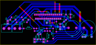
I am sorry but I don't really like your PCB layout.
I am sure others have other opinions but for me a good PCB layout follows the rules below:
1: Differential signals and power supply lines are always routed in close pairs.
2: Input and output are separated
3: High current signals (PSU and OUTPUT) close together, staged with multilayers
4: PSU capacitors close together, and PSU routing on the left side, line input routing on the right side (keep them separate)
5: Grounding, In case of star-ground, route each ground-trace separate back to the common ground point (avoid serial grounding). In case of a ground-plane, They can work really well, but only if you do it right, and in most cases to do it right you need a 4 layer board. A ground-plane should be unbroken (no traces or lines) and on a layer of it's own all reserved to function as ground-plane. Then you must place components very careful and study the current return loop of each part, and keep those currents in mind when you place components.
In your particularity case, Your low level line input signals are all buried in a loop of high current signals. A better choice would be to route the PSU all on the right side, and feed the chip from the right side. The audio line signal on the right side. The outputs in the middle in front of the chip. Please take a look here for an example: sjostromaudio.com - QRP02 The SMD Gainclone - high performance mono power amplifier
Get rid of the serial ground polygon. This doesn't work as real ground-plane. Make a common ground point, and route each ground trace separate to here. PSU capacitors should be close together, and not with a long ground joint between them.
Good luck!
With kind regards,
Bas
Yeah Sebastian, i got your points
In fact i do not want to use a double layer PCB cos my man cannot put through a good pcb with two sides, i generally construct my designs on a single layer and if necessary i use jumpers (which are seen as top layer of pcb in the pic)
Then i will give it another try and post it.
Meanwhile, i will of course accept any other comments")
In fact i do not want to use a double layer PCB cos my man cannot put through a good pcb with two sides, i generally construct my designs on a single layer and if necessary i use jumpers (which are seen as top layer of pcb in the pic)
Then i will give it another try and post it.
Meanwhile, i will of course accept any other comments
Yeah Sebastian, i got your points
In fact i do not want to use a double layer PCB cos my man cannot put through a good pcb with two sides, i generally construct my designs on a single layer and if necessary i use jumpers (which are seen as top layer of pcb in the pic)
Then i will give it another try and post it.
Meanwhile, i will of course accept any other comments
Okay,
In that case you just need clever routing. Take your time to consider all points. For sure in your case use a star ground then. Even though you are using a single layer PCB with jumpers, you can still keep the PSU lines together and feed it from the left side, and feed the line level from the right side.
Good luck!
With kind regards,
Bas
Hi,1: Differential signals and power supply lines are always routed in close pairs.
this is important.
Both in the flow and return wires to the PCB and in the flow and return traces carrying currents across the PCB.
for effective attachment of the heatsink the Chipamp should be at or near the edge of the PCB.
The decoupling caps C6 C1 have a very dirty current between their Zero Volt pins.
Do Not place any Ground Reference on this linking trace.
Why is V- separate from V+?
Look at the route from pin4 to C5 to C2 to pin9. That route must be at least 10times the length of the route from pin 4 to pin 9. That type of routing can be avoided by using the single amp version, lm3886.
V- is a bit apart from V+ so that i can keep up with star ground with the single layer PCB, the real distance is 1 inch (2.54 cm)
You are correct that C1 & C6 are very distant, for that reason, i placed C2, C3, C4 and C5 as close as possible to IC, they have the values 10u and 100n.
I did not understand the idea behind the route length constraint you said, can you explain the reason please?
Meanwhile i will try a bridged version
- Status
- This old topic is closed. If you want to reopen this topic, contact a moderator using the "Report Post" button.
- Home
- Amplifiers
- Solid State
- LM4780 stereo Power-amp PCB design