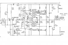
I have a Traynor Mono Block II bass guitar amp that has a tendancy to fry power transistors. I've talked with several others that have told me that this is a common problem with this model. The transistors are getting more difficult to find and I would like to rebuild the power amp section into something more reliable. The amp is rated to produce 325 Watts at 2 Ohm load and it uses + - 56V rails. I don't care if I end up with an amp that is that powerful but I would like to at least end up in the 150W @ 4ohm range. What power output circuit would you recommend for this rebuild?
I've build many tube amps and a lot of solid state preamps and signal processors but this will be my first solid state power amp.
I've build many tube amps and a lot of solid state preamps and signal processors but this will be my first solid state power amp.
Attachments
2N5630? That may have been a good choice in 1976, but the common MJ15024 would drop right in its place. DOn't mix, replace the whole group of four.
I am assuming those, since the 2N3773s in the later version are not hard to find.
Running a 4 ohm load, and thus drawing half as much power, would make the amp work a lot less harder than at 2 ohms.
I don't know why they could be prone to blow ups, but the bias circuit is extremely crude - a single dual diode. I am sure it works as well as they intended when everything is fine, but if the junction drop voltages in that part start to climb, then idle current goes up and up.
Once repaired, let the amp sit there powered up and idling. Does the heat sink get hot under those conditions?
Yes, I can find 2N3773 but it usually pops the SJ5480 (Q9) also. If I use the 2N3773 can I use it's compliment, the 2N6609 for Q9? What should I use for Q1 and Q9 if I use the MJ15024? Also, what do you suggest for improving the bias circuit?
I never run it down to 2 ohm load, almost always 4 ohm and often only 8 ohm.
Once I get it rebuilt, I'll let it idle a while and see how hot the sinks get.
Thanks for your reply Enzo.
I never run it down to 2 ohm load, almost always 4 ohm and often only 8 ohm.
Once I get it rebuilt, I'll let it idle a while and see how hot the sinks get.
Thanks for your reply Enzo.
you may as well built a more decent VBE multiplier arround this circuit that will provide by far better thermal stability...
mod like the above will need verification with scope and generator to make sure that nothing oscilates from the change of the transitors or the wiring issues that are often a problem with this setups
adding decoupling 100MF/100 volt next to the transistors from rail to ground will also add something to the total performance but it needs to be done carefully
other than the above i like this circuit ....
regards sakis
Can you give me an example for the VBE multiplier?you may as well built a more decent VBE multiplier arround this circuit that will provide by far better thermal stability...
What do you mean by "carefully" with respect to adding the 100MF/100V caps?adding decoupling 100MF/100 volt next to the transistors from rail to ground will also add something to the total performance but it needs to be done carefully
This amp may be an older design, but it still has a very good reputation among bass guitar players for having a very good tone, response and power. I'm glad a couple of you think it's worth rebuilding instead of gutting and starting over. I'll pop it open and take pictures so you can see how it's laid out.other than the above i like this circuit ....
i am not aware how the circuit is builted .... i think its made with cables from pcb to transitor outpouts ...if there decoupling is needed then next to rails and close to transitors you need a ground cable ...tha can cause complications
then again pictures will help
a decent vbe multiplier is made out of a proper tranistor that can easly be a bd 135 a trimer and few resistors ... actually your diodes might work better but have noa adjustement and also i am not really sure that have perfect thermal and mechanical contact with the heatsink.... again some picture might help
another thing that i could try to is to convert the circuit to a coplementary amplifier than a quasi .... easy task but yet again needs to be verified and checked very properly before put to work ...
kind regards sakis
The complement of the MJ15024 is the MJ15025.
I am not into redesigning the amp, others can do that. I have no improvement ideas for the bias, Sakis is making a suggestion. My concern is that if the amp is eating transistors, CHECK that dual diode to see if it is slipping.
You should be able to use the MJ15024 exactly as you would the 2N3773. SO if they use 2N3773 for both the outputs and the + side driver, The MJ15024 would work for both applications as well. And the MJ15025 on the V- side.
They show a 2N3773 as the driver (Q1) in the later amp, is that right is it a TO3 case device?
The bias diodes are fine, it is class B underbiased and if you want to retain the classic design leave that alone.
I'd have to wonder if the CFP side is oscillating and causing the driver failure, if not the failure in the first place. Do both output devices fail when it goes?
If you want to go to a modern device I'd make it an MJ21194G.
Replace all the electrolytic caps due to age.
Check all the diodes. Check R29 if it is bad also replace C11.
Test Q6 and Q7.
Last edited:
I can get the MJ15024G and MJ15025G from mouser. Might be best just to replace the diodes too. Hopefully the newer transistors will hold up better.
to my understanding this approach is wrong .... there is no "drop in" replacement transistors any variation an the transitor specs will have grate effect on the bias and total performance
presumambly the double diode will be almost unobtainable so dont bother looking for it ...
to my opinion any change will need to be verified by instruments
and finaly redesign from quasi to complementary will not happen by replacing the lower transistor of course it will take more than that ...
simple as that if you have approach to instruments and procedure go ahead play but verify your work ...if not just replace the broken and any capacitors that might be old and moove on ...
regards sakis
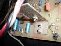
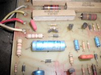
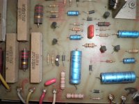
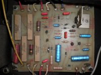
OK, I opened it up and found a couple things. I wasn't the one that replaced the transistors when it popped them last time and I see they were replaced with something else. The quad of transistors used last were 2N3055 and the drivers used were MJ15015 and MJ15016. I was told that the time before when this happened, it popped the drivers as well but I haven't checked them.
The previous owner had someone replace the transistors 3 times in about 2 years timeframe. He got tired of messing with it and when it popped them last, he just gave it to me.
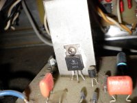
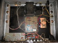
As I mentioned before, I'm new to solid state power amps but I have considerable experience with tube amps and sold state signal processors. I've added a few pics of the inside for reference.
I've not lifted the pcb to follow traces but I don't see where that 8213 is shown on the schematic.
The previous owner had someone replace the transistors 3 times in about 2 years timeframe. He got tired of messing with it and when it popped them last, he just gave it to me.
As I mentioned before, I'm new to solid state power amps but I have considerable experience with tube amps and sold state signal processors. I've added a few pics of the inside for reference.
I've not lifted the pcb to follow traces but I don't see where that 8213 is shown on the schematic.
Attachments
It would be a gross understatement to say that MJ15015 and MJ15016 are a poor choice for drivers.
Something is strange about what is going on here; the amp has output protection yet the output devices are failing. Now, 2N3055s are also very poor choices for the output devices but what causes it to fail the first time from the factory, hopefully with good parts? The output protection is not just current limiting, it is actually VI limiting which is good since it provides a lower current limit under short circuit conditions but a higher current limit into normal loads. This output device Vce dependent current limiting is provided by the 1.8K resistors R9 and R16, however I believe that they are too small and may cause the protection devices to have their B-E junctions reverse biased beyond their allowable rating. Perhaps the protection devices fail and then there is no output protection. It would be very interesting to remove and test them. let us know what you find.
Another consideration is the 22uF's C5 and C7 on the protection devices these will make them slower to respond and hopefully avoid oscillation - perhaps it is too slow and simply allows the output devices to fail. The time constant is not so straight forward to estimate due to the non-linear B-E junction of the protection transistor. You could get the amp working and then look at the protection circuit operation on a scope and adjust the cap value if needed.
There is a good chance that the output devices are fakes, and 2N3055s are not a good choice anyway ... so I would start by pulling the outputs, drivers, protection transistors and testing them, note where each 2N3055 comes from in the circuit - tell us what you find.
You will probably want to pull the VAS Q8 and its protection transistor Q12 and test those also.
In order to avoid blowing up more outputs as you bring it back up, you will want to current limit the supply lines with resistors (10 or 100 ohms) so disconnect the main supply from the amp.
You will want to use the power supply to test the new outputs that you get for Vceo to help weed out fakes (unless you are absolutely sure of your source) so having it disconnected is good.
You should be able to test many of the resistors and diodes without removing them just by having these parts out.
Here is another amp repair that I helped with and there were issues with fake replacement parts - it is very common:
http://www.diyaudio.com/forums/solid-state/157682-another-high-dc-adcom-gfa-555-a.html
Last edited:
OK, more information. I pulled the transistors and found the following:
Q1, transistor failed, no conduction, all pins check open
Q2, transistor failed, B to C diode check shows conduction both ways, B to E checks open both ways. Also socket toasted and R5 appears to be totally missing, not burned up but forgotten when socket replaced at some time.
Q3, transistor failed, no conduction , all pins check open
Q11, transistor failed, no conduction , all pins check open
Q10, transistor failed, all pins conduct, both direction
Q9, transistor failed, no conduction , all pins check open. Also this transistor was missing it's mica insulator, attached directly to heat sink with thermal paste, would make collector attached to chassis. Wonder if amp popped immediately upon power up last time.
Edit: I looked at Q2 socket more and it's possible that R5 vaporized, but I don't find any part of it. Not sure if it was there or not but it's gone now.
Nothing else appears to be burned up. haven't checked anything else other than detailed visual except I do find that rail voltages are fine.
Last edited:
Ok, checking with them in circuit, ALL of the power amp board transistors check showing zero conduction from all pins in all directions. So I'm assuming it popped them all this time. I guess I need suggestions for replacement parts there as well. No parts look toasted but a couple of the 1/2 watt carbon films look a bit darkened. I'll check them in circuit too. I need more light and a magnifying glass to see exactly what Q8 is.
The part that I was asking about earlier and calling a 8213 is actually the Q8 and it looks like a TIP 41. There is a picture of it posted earlier and I can't tell for sure if it's a TIP41 or TIP47 but it looks more like a TIP41 to me.
Edit: looked more closely, I am sure it's a TIP41C.
Edit: looked more closely, I am sure it's a TIP41C.
Last edited:
Have you decided if you want to rebuild it as fully complementary?
It is interesting because as it is now as a Quasi Comp design one side is CFP and the other EF. CFP gives you excellent current drive but is prone to instability, and the long wires from the driver board only make it worse, so if you want fully comp I'd probably go with both sides being EF.
I can understand wanting to keep it original as Quasi Comp also.
I'd guess that the original drivers were something like MJ4248/MJ4238: 150V 8A 90W 20 MHz hfe = 40 at 3A
Doubt that you can get them anymore and I don't know of any metal case TO3s that are similar and available today.
There are Fairchild plastic TO3P types that I believe will drop in if you bend the pins and hook up the center collector lead with a ring lug to the screw: FJAF4210YTU, FJAF4310YTU
The only other obvious choice are the MJE15030/31 but they are in a TO-220 case and you would have to see if the leads could be made to fit the socket.
Since I now am facing the situation of ALL the power amp section having blown transistors. I'm very keen on the idea of rebuilding as fully complementary. As mentioned before, I'm still coming up to speed on solid state power amps so I want to do something that is tried and true with 56V rails and knowing I'll have long wires from driver to transistors. Do you have a suggestion for a fully comp design? The heat sinks have flange sections that easily can accept a TO220 package so it doesn't have to stay metal case transistors. I don't want to reinvent the wheel, just find the wheel that fits.
the original amplifier could work perfectly if you just need simply to upgrade some parts but with out messing up with the topology that will need instruments to verify
the amplifier has only couple of mistakes as i can see from photos ...
1the double diode string canot be placed on the pcb it needs to be placed in thermal contact with the heat sink
EXPLAIN
bias of the amplifier come from there , as amplifier operate outputs are getting warmer , without sensing ( from the diodes ) of how much warmer ( this what the diode can do :sense the temperature and decrease bias ) then as amp gets warmer bias without sensing increase till distruction of outputs ....phenomenon called """Thermal runaway""
2Wiring
wiring between pcb and outputs is horrible base /emmiter / collector wires cannot be twisted that will cause some mess up ...also need to be thicker but most importand is to have if possible the same distance from pcb .... the second is less importand if cables are thicker
simple solution
--- get proper semis ( better than the existing ) drivers/ outputs
--- Do some mechanical work , get proper heatsnink , locate all transitors in the one side , ensure that they breath properly, do proper wiring , install diode string somewhere on the heatsink that can realy sense temperature ( or replace withtransitor based sensor ) and your amp will rock for almost 30years more
regards sakis
Last edited:
- Status
- This old topic is closed. If you want to reopen this topic, contact a moderator using the "Report Post" button.
- Home
- Live Sound
- Instruments and Amps
- Rebuilding the Traynor Mono Block II