Hello,
I have a question about correctly biasing a mosfet for class-a operation. I am a relative newbie, so sorry if I am not interpreting the data sheet correctly. Thats why I need you guys.
Specifically, I am using Nelson Pass' "balanced zen line stage" as my input stage.
http://passdiy.com/pdf/balzenpre.pdf
I'll be using the IRF510 FET:
http://www.vishay.com/docs/91015/91015.pdf
This stage must take the signal from my DAC, which has a rather hot 2.75Vpp single ended, 5.5Vpp balanced signal. At the output of the zen stage, I need about 20Vpp. So this is only roughly 4X gain.
In Nelson's article, he has the source of Q1 and Q2 set to around -3.5 to -4V.
In looking at the Vgs vs Id graphs on the data sheet, this makes sense if the input signal is in the 1Vpp range. But in my case, where the signal driving the gate is relatively large, what to do?
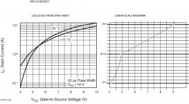
The graph in the data sheet has Id drawn in log scale, so I manually redrew it in a linear scale, so I can see the curve correctly (attached).
What I see is a large hump at 5V which is where I presume the FET goes from linear region to saturation? Because my input signal spans almost 3Vpp, this is larger than the whole linear region.
So my choices, in my mind, are to voltage divide the original signal down to around 1Vpp, and set the Source to around -4V. Or I could use the full 2.75Vpp input signal as is, and bias the source pin to -6.5V or so. Here I presume I would be running the FET in saturation mode, which according to the graph, still has a very nice 'linear' look to it.
Are these observations, assumptions correct? Am I interpreting the graph correctly? Could someone give me some informed advice?
Thannks
I have a question about correctly biasing a mosfet for class-a operation. I am a relative newbie, so sorry if I am not interpreting the data sheet correctly. Thats why I need you guys.
Specifically, I am using Nelson Pass' "balanced zen line stage" as my input stage.
http://passdiy.com/pdf/balzenpre.pdf
I'll be using the IRF510 FET:
http://www.vishay.com/docs/91015/91015.pdf
This stage must take the signal from my DAC, which has a rather hot 2.75Vpp single ended, 5.5Vpp balanced signal. At the output of the zen stage, I need about 20Vpp. So this is only roughly 4X gain.
In Nelson's article, he has the source of Q1 and Q2 set to around -3.5 to -4V.
In looking at the Vgs vs Id graphs on the data sheet, this makes sense if the input signal is in the 1Vpp range. But in my case, where the signal driving the gate is relatively large, what to do?
The graph in the data sheet has Id drawn in log scale, so I manually redrew it in a linear scale, so I can see the curve correctly (attached).
What I see is a large hump at 5V which is where I presume the FET goes from linear region to saturation? Because my input signal spans almost 3Vpp, this is larger than the whole linear region.
So my choices, in my mind, are to voltage divide the original signal down to around 1Vpp, and set the Source to around -4V. Or I could use the full 2.75Vpp input signal as is, and bias the source pin to -6.5V or so. Here I presume I would be running the FET in saturation mode, which according to the graph, still has a very nice 'linear' look to it.
Are these observations, assumptions correct? Am I interpreting the graph correctly? Could someone give me some informed advice?
Thannks
Attachments
Based on my experience, if Vgs is too high, it is true if it can go to saturation for certain MOSFET, but not for the other MOSFET (higher Id and VGs saturation). If this is for linestage, then the proper handling may be to reduce the Vgs bias. Usually around 2V is enough to be in linier mode (depends on MOSFET). If you need higher Vgs saturation, may be you can try higher MOSFET like IRFP 240. But this is normally for power amp, not linestage. Or use lateral, with lower Vgs.
Ervin L
Ervin L
The graph in the data sheet has Id drawn in log scale, so I manually redrew it in a linear scale, so I can see the curve correctly (attached).
What I see is a large hump at 5V which is where I presume the FET goes from linear region to saturation?
Your re-drawing of the curve has distorted it, so the 'hump' you're seeing is an artifact of that. The ten lines below the 1A level need to be compressed down to one line as that range is from 0.1A to 1A. As it is now, the lower half of your graph has 0.1A steps and the upper half, 1A steps.
Mosfet biasing
Ahh, yes you are right about that. Thanks for catching my mistake. It is difficult to see the linearity of the gain when they use the log scale. Any tricks to eyeballing this as I browse for appropriate FET's?
Your re-drawing of the curve has distorted it, so the 'hump' you're seeing is an artifact of that. The ten lines below the 1A level need to be compressed down to one line as that range is from 0.1A to 1A. As it is now, the lower half of your graph has 0.1A steps and the upper half, 1A steps.
Ahh, yes you are right about that. Thanks for catching my mistake. It is difficult to see the linearity of the gain when they use the log scale. Any tricks to eyeballing this as I browse for appropriate FET's?
Any tricks to eyeballing this as I browse for appropriate FET's?
I can't see any reason not to feed the full 5.5p-p signal into this circuit. The -4V bias is only the quiescent (no signal) condition and its determined by how much current you want through the FET in this state (set by the 2 750R resistors). As you apply more voltage, the source voltage will follow the input as its effectively a source follower, so it will range from -1.25V to -6.75V. If your supply rails can handle this (seems they'll be high, around 80V?) then no problem as the signal is only a small fraction of the DC bias.
In Nelson's article, he has the source of Q1 and Q2 set to around -3.5 to -4V.
In looking at the Vgs vs Id graphs on the data sheet, this makes sense if the input signal is in the 1Vpp range. But in my case, where the signal driving the gate is relatively large, what to do?
Thannks
Hi
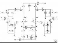
I think you may be mis-understanding the relationship of Vgs and Id relative to the circuit. The source voltage is not fixed. It appears in fig 3, Id bias is 28.2V/750R or 38mA. For a 20Vp output signal, the change in Id is +/- 20V/750R or ~27mA. So the AC load line plots (Id vs Vds) between 11mA and 65mA, with Vds of 14V (@65mA) to 54V (@11mA). A current swing of 54mA is not going to require a very large change in Vgs. The source voltage will follow the signal voltage on the gate, less this small change in Vgs. Vgs threshold is not very relevant, one can simply adjust a resistor value to make the difference for any fet of suitable SOA. IRF610 is a typical hex type switching fet. They are all similar.
As a side note, I find it easier to understand FETs by the variables relationship to transconductance (Gm) as opposed to current flow as they are voltage controled devices. BJTs are current controled and so it is easier to anylize the circuit using current flow.
")

BJTs are current controled...
A very popular myth but in reality (physics) they're exponentially voltage controlled. MOSFETs are square-law voltage controlled.
true, but in anylizing a circuit, I find it is easier to think of them as such.
I tend to analyse them assuming they've got 0.6-0.7V between the base and emitter, then use gm (as you suggest) to find out what the currents might be. hFE is one of the parameters which is not very tightly controlled in bipolar transistors, usually it has quite a broad spread and, especially for power devices, its highly dependent on Ic. gm in bipolars is much easier to 'get' as its only a function of the collector current, not the geometry as is the case in MOSFETs.
Hi
I think you may be mis-understanding the relationship of Vgs and Id relative to the circuit. The source voltage is not fixed. It appears in fig 3, Id bias is 28.2V/750R or 38mA. For a 20Vp output signal, the change in Id is +/- 20V/750R or ~27mA. So the AC load line plots (Id vs Vds) between 11mA and 65mA, with Vds of 14V (@65mA) to 54V (@11mA). A current swing of 54mA is not going to require a very large change in Vgs. The source voltage will follow the signal voltage on the gate, less this small change in Vgs. Vgs threshold is not very relevant, one can simply adjust a resistor value to make the difference for any fet of suitable SOA. IRF610 is a typical hex type switching fet. They are all similar.
As a side note, I find it easier to understand FETs by the variables relationship to transconductance (Gm) as opposed to current flow as they are voltage controled devices. BJTs are current controled and so it is easier to anylize the circuit using current flow.
I think you are right. I am misunderstanding the relationship of Vgs and Id relative to the circuit. And you are right- it makes perfect sense that the source is not fixed, now that you mention it. I need to hit the books to follow the rest of your statement though. I have the Art of Electronics, and I'll have to dig online a little further. In the past, my only experience w/ mosfets was to use them as switches, not as gain devices, so this is a bit new.
I look at both FETs and BJTs as transconductance devices. In simple language change the input voltage and the current passing changes with that input increment.
Yup, I get that part.
Its understanding the biasing, reading the curves on the data sheet, and being able to some proper calculations that is my next stop.
Thanks for everyone's posts- you caught a couple of my misunderstandings right off the bat.
The best and easiest to see, understand
is when we use one Practical circuit as example.
Refering to a certain case, circuit we can suggest changes to resistor R1 or R2
and discuss the result.
Theoretical, abstract discussions tend to be at least twice as long
to teach the one and same thing.
And as with most things, the practical specific case
is what determine how the parameters will work + the limits for operation.
The best and easiest to see, understand
is when we use one Practical circuit as example.
Refering to a certain case, circuit we can suggest changes to resistor R1 or R2
and discuss the result.
Theoretical, abstract discussions tend to be at least twice as long
to teach the one and same thing.
And as with most things, the practical specific case
is what determine how the parameters will work + the limits for operation.
Good point. Actually it reinforces how I think I have learned anything in electronics.
Lets look at the pass circuit again (attached). If we could just look at the left half of the circuit, how were the values pf R1, R3, R4 determined?
Furthermore, what are we looking at on the datasheet of the FET, that allows us to make these design decisions.
http://www.vishay.com/docs/91023/91023.pdf
Attachments
r1,3,4 are based on design currents.
Look at the circuit, as a first guess set r16,17 to 0r0.
Now use the design voltages and the resistor values shown to determine the currents.
Now imagine you have a datasheet in front of you and previous experience of using this device. You look at what you think would be a suitable operating current. Check the dissipation to ensure sufficient reliability.
Set your target voltages.
Using voltages and currents determine the resistor values.
You'll find that that first stab at setting r16,17 to 0r0 introduced a voltage error of <900mVdc
Last edited:
Lets look at the pass circuit again (attached). If we could just look at the left half of the circuit, how were the values pf R1, R3, R4 determined?
Here are the steps I'd take if I was designing this circuit.
First, I'd want to estimate how much power I could afford to dissipate in the FET. This depends on whether I have a heatsink and what the thermal resistance of that heatsink is. This allows me to set a power budget based on the maximum temperature of the heatsink. Let's suppose that my heatsink calculations mean the FET's going to be fine below 12W dissipation.
Next stage, what's the maximum current I can tolerate through the FET if all the power supply voltage (120V) is across it? This is just a worst-case figure, to allow me to get the feel of the circuit - here its (from I = P/V) 100mA.
Having set the boundaries, I'll next look at the datasheet fig3 to see what VGS (gate-source voltage) I can expect at 100mA. This turns out to be about 4V - again, its a maximum figure because the 100mA is a maximum. Note that this figure is strongly temperature dependent for the FET, but given the high power supply voltages in comparison to it, we don't need to be worried overly much about that.
Now I'm in a position to estimate the various circuit voltages. The gate will be at 0V and the source at -4V. Given the source voltage, I now choose what the quiescent current will be through the FET in selecting the values of R3 and R4. I am guessing there are two resistors here because they'll get quite warm. We have a voltage across the pair of (60-4) = 56V. The series value is 1500 ohms setting the bias at 37.3mA. Notice that this gives me a very big safety margin - its only about 1/3rd of the maximum. Dissipation in each resistor will be I2R = (0.0373^2*750) = 1.05W so we really need to specify 2W parts as a minimum. Preferably mount them a fair distance from any electrolytic caps too.
Having chosen the source resistors, its only necessary to choose the drain resistor R1, depending on how much gain we want and what output voltage levels are acceptable. Note these two parameters are strongly interlinked. Because audio signals are generally symmetrical, we want as much freedom above the voltage as below it. This is what leads to the choice of 30V as the output quiescent level. Given the drain resistor will drop 30V, its simple to calculate its value as (30/0.0373) = 804R. We're already using some 750R so its not much of a compromise to use one of these, the dissipation is the same as for the source resistors so it also needs to be 2W.
Now, looking at the schematic again, I see there are 22R resistors in series with the 60V power supply. So these will change the circuit voltages somewhat. I had no idea how much before I calculated the FET currents, but it was necessary to start somewhere. Now then, a quick sanity check to see how much difference those resistors are making. We have two FETs running at 37.3mA which is 74.6mA, this current through 22R gives a voltage drop of 1.64V. Not very significant in the scheme of things, so I don't need to redo my resistor calculations.
This is how I do it.
1. You have a power supply, suitable, with Voltages.
2. For each stage, each transistor, I decide a working Current.
What current I can find out using Datasheet.
It is a current at where the transistor works well for the job.
3. By using resistors I set those currents I want.
I use SPICE Simulations. So, assuming I have good models,
I can change resistors and measure currents.
And also see if circuit as a whole probably will work well.
With practical real circuits you can come a long way using multimeter.
Oscilloscope is absolutely best. Can see more than multimeter.
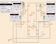
I have setup your circuit in SPICE.
Input signal is 2.75Vp + 2.75Vp
Output is 10Vp + 10Vp (same as 7.071Vrms at each output)
While testing it shows that IRF510 has less than half THD% distortion than original IRF610.
At least those SPICE models I have tells so.
I have replaced the original 124 Ohm resistor with 330 Ohm + 200 Ohm trimmer.
This way you can adjust to get the gain around x4.
The gain is a bit load dependent.
With only those 100k at output the gain is higher.
But putting a load, 5k in my circuit, the gain will be lower
so you need adjust the 200 Ohm trimmer a bit to compensate.
The gain depends on R1 750 Ohm / the impedance below the source.
Load resistor 5k will be parallel with the R1 and give a resulting impedance
at the DRAIN of ~652 Ohm instead of 750 Ohm.
This means gain will be only ~86% of the teoretical value.
Finally.
At output swing of 10 Volt peak with only 0.011% THD
this is a remarkably good circuit! Without global feeedback.
Well done Mr Nelson Pass
/lineup
Attachments
- Status
- This old topic is closed. If you want to reopen this topic, contact a moderator using the "Report Post" button.
- Home
- Amplifiers
- Solid State
- How to bias mosfet in Class-A