Hello Bob,
I bought your book and I'm thrilled. Even as a German I was able to understand the most immediately. The book has saved me a lot of work and explains many things I still wanted to know.
Thanks")
Hi moschfet,
Thank you for your very kind words. I'm glad you enjoyed the book.
Cheers,
Bob
Hi Bob,
Once again, many thanks for your excellent book.
I have a quick question I'm hoping you or someone else on the forums might be willing to answer. In your book you discuss several ways of implementing thermal compensation for power MOSFET amplifiers, mentioning that the standard Vbe multiplier will overcompensate. You then provide an array of slightly more complicated solutions.
Something I am wondering is whether a simple Vgs multiplier using a small mosfet could be used instead? What are your thoughts?
Your advice is appreciated!
Regards,
Greg.
Hi Bob,
Once again, many thanks for your excellent book.
I have a quick question I'm hoping you or someone else on the forums might be willing to answer. In your book you discuss several ways of implementing thermal compensation for power MOSFET amplifiers, mentioning that the standard Vbe multiplier will overcompensate. You then provide an array of slightly more complicated solutions.
Something I am wondering is whether a simple Vgs multiplier using a small mosfet could be used instead? What are your thoughts?
Your advice is appreciated!
Regards,
Greg.
Hi Greg,
This is an interesting idea. I must admit that I have not tried it, or given much thought to it.
If it is used in a MOSFET amplifier where the VAS drives the MOSFETs directly (i.e., no driver), then I'm guessing it might work quite well.
If it is used in a MOSFET amplifier where BJT drivers are used, then a more complex arrangement might be needed if the Vbe TC of the BJT drivers is to be properly taken into account. Taking the BJT TC Vbe into account may also depend on whether the BJT drivers have their own heat sinks or whether they are mounted on the main heat sink along with the power MOSFETs.
Also bear in mind that the type of MOSFET has a bearing on all of this. Lateral MOSFETs are often biased at a point close to where their TC is nearly zero. Vertical MOSFETs, the main context in which I was discussing bias spreader temperature compensation, have a positive temperature coefficient of Id vs temperature that is big enough to need some temperature compensation.
Cheers,
Bob
Thanks Bob.
The circuit I have in mind is a vertical fet output with folded drivers as per your figure 11.16. As I understand it, this pretty much removes the Vbe temperature variations of the drivers from the equation and leaves us with only that of the power fets. So in this situation the Vgs multiplier might be ideal?
Thanks for your advice.
Greg.
Thanks Bob.
The circuit I have in mind is a vertical fet output with folded drivers as per your figure 11.16. As I understand it, this pretty much removes the Vbe temperature variations of the drivers from the equation and leaves us with only that of the power fets. So in this situation the Vgs multiplier might be ideal?
Thanks for your advice.
Greg.
Hi Greg,
This is largely true, but not completely true. The folded EFs, Q1 and Q2, introduce a Vbe TC, but note that it is of opposite sign to that we normally must consider with non-folded drivers. This is a nice feature and gets us closer to where we want to be. However, Q1 and Q2 don't warm up the same (or as much) as the power MOSFETs, unless they are mounted on the main heat sink. So a Vbe multiplier bias spreader transistor may still be needed to be mounted on the heat sink. It may not need to have as much TC-inducing "strength", so it may want to be in series with a diode or two in the bias spreader that are only exposed to board ambient.
See Figure 11.8 for some useful bias spreader arrangements. See also Figure 14.11 for some useful bias spreader arrangements as well.
Cheers,
Bob
Bob,
I recently measured some large mosfets from Fairchild and found the tempco to be 6mV/C for quiescent currents up to 200mA.
As you say, and Greg and I are both working on this together in fact, the bipolar drivers would each compensate to pull back the combined 12mV/C of the large mosfets a little, but OTOH they are running at reasonably constant power and so merely reach equilibrium after twenty minutes or so and likely would not be on the output heatsink metering temperatures anyway.....
So, if we assume that around (4.1 x 2) - (0.65 x 2) = 6.9V is required at the bias generator, then another effective solution using a cheap bipolar device as bias control might be to devise a Vbe multiplier that attaches atop one of the output devices - say a BD139 with 1.8mV/C, and set it to around 11mV/C by selecting 5 times Vbe between CB - 3.15V, and giving a total C to E voltage of 3.8V. This would typically mean Rbe of say 680R, and Rcb of 3k3, npv. I would assume at least 15mA flowing through the Vbe multiplier. The difference between the required bias, 6.9V, and 3.8V of the tailored Vbe multiplier could then be taken up with a simple resistor, in this case of 206R, obviously a pot for adjustment.
Is this on the right track?
Thank you very much for your time. I have found the tempco of a large mosfet at low bias currents to be an accident waiting to happen; they can get out of control very quickly.
Cheers,
Hugh
Last edited:
Bob,
I recently measured some large mosfets from Fairchild and found the tempco to be 6mV/C for quiescent currents up to 200mA.
As you say, and Greg and I are both working on this together in fact, the bipolar drivers would each compensate to pull back the combined 12mV/C of the large mosfets a little, but OTOH they are running at reasonably constant power and so merely reach equilibrium after twenty minutes or so and likely would not be on the output heatsink metering temperatures anyway.....
So, if we assume that around (4.1 x 2) - (0.65 x 2) = 6.9V is required at the bias generator, then another effective solution using a cheap bipolar device as bias control might be to devise a Vbe multiplier that attaches atop one of the output devices - say a BD139 with 1.8mV/C, and set it to around 11mV/C by selecting 5 times Vbe between CB - 3.15V, and giving a total C to E voltage of 3.8V. This would typically mean Rbe of say 680R, and Rcb of 3k3, npv. I would assume at least 15mA flowing through the Vbe multiplier. The difference between the required bias, 6.9V, and 3.8V of the tailored Vbe multiplier could then be taken up with a simple resistor, in this case of 206R, obviously a pot for adjustment.
Is this on the right track?
Thank you very much for your time. I have found the tempco of a large mosfet at low bias currents to be an accident waiting to happen; they can get out of control very quickly.
Cheers,
Hugh
Hi Hugh,
Yes, the TCvgs of vertical MOSFETs you quote of about 6 mV/C is about what I have seen over a long time. And yes, if it is not compensated it can be a disaster waiting to happen. Those accustomed to using lateral MOSFETs must be especially mindful of this difference. The zero TC crossover point for large vertical MOSFETs is on the order of several amps.
Placing the portion of the Vbe multiplier on the case of the power MOSFET definitely helps get closer to the real heat source. The thermal resistance of the insulator in general (i.e., even for BJT amps) interferes with good thermal tracking, as does the fact that heat sinks are far from isothermal.
As I mentioned in my MOSFET power amplifier paper with EC, vertical MOSFETs are far more temperature stable when reasonably compensated than bipolars. In a sense, I guess, they lie between BJTs and laterals. I was able to show this with a plot of bias current vs time after a large change in operating signal power level.
Of course, the availability of ThermalTrak BJT transistors makes it possible to build BJT amplifiers with thermal stability just as good as those using vertical MOSFETs (maybe even better, since the sensing diode in the ThermalTraks is thermally closer to the BJT junction (whose temperature is what really counts).
You are definitely on the right track. The whole thermal circuit of temperature compensation of any output stage is so complex that some experimentation and lab measurement is still important in evaluating and establishing thermal stability.
BTW, I usually believe that we must consider both static and dynamic thermal stability. If you turn on an amplifier with no signal and plot quiescent bias as a function of time, you are evaluating static bias stability. Similarly, If you do the same with the amplifier passing a signal and putting some power into the load, you are still largely evaluating a quasi static version of bias stability.
Dynamic bias stability defines how the amplifier bias current reacts to large changes in power dissipation as a result of signal. For example, if you let the amp warm up with no signal, measure quiescent bias, then run it at 1/3 power for 10 minutes, then remove signal and measure quiescent bias as a funtion of time, you are evaluating dynamic bias stability.
The second case cited above, where the amp is turned on with signal applied and samples of bias current are taken versus time, has somewhat a combination of static and dynamic bias stability aspects to it.
Cheers,
Bob
Hi,
I am refering to page 306, figure 14.18c with the voltage across each junction deduced from the values shown at left.
Currently, on figure 14.18c, the voltage across R1 is about an 1.4 V determining a current about 0.7 mA in R1 and R2. It is indicated as being 1 mA. With 0.7 mA, the calculated bias spreader votage is about 3.6 V
Decreasing R1 from 2200 Ohm to 1300 Ohm just as it is in figure 14.19a, this should give a current of 1 mA and a bias spreader voltage as 4.2 V, as written.
Regards.
Hi,
I am refering to page 306, figure 14.18c with the voltage across each junction deduced from the values shown at left.
Currently, on figure 14.18c, the voltage across R1 is about an 1.4 V determining a current about 0.7 mA in R1 and R2. It is indicated as being 1 mA. With 0.7 mA, the calculated bias spreader votage is about 3.6 V
Decreasing R1 from 2200 Ohm to 1300 Ohm just as it is in figure 14.19a, this should give a current of 1 mA and a bias spreader voltage as 4.2 V, as written.
Regards.
Hi forr,
Yes, it looks like you are right. Good catch. I deeply appreciate any errors in the book being brought to my attention.
Cheers,
Bob
1.4V bias circuit for Diamond Buffer Triple employing NJL TT devices?
I have been having a hard time putting together a bias spreader that could correctly track the 2.1mV/C NJL Vbe with the 1.7mV/C ThermoTrak diode tempco for a triple output stage that has a diamond buffer as its pre-driver and driver, which requires a bias voltage of about 1.4V. This 1.4V really is a very small play ground that doesn't house many p/n junction drops. So after some head scratching I came up with a circuit that seems to be able to serve the purpose.
The circuit diagram is in the attached pdf. It uses an op amp MAX4289 that works on as low as 1.0V supply and swings rail-to-rail. I set it up to have a gain of 2.5 to derive a 4.25mV/C for the two b-e junctions of the output transistors from the TT diode's 1.7mV/C tempco. R6 is the bias trim pot. It sets a bias current in the TT diodes so as for them to come up with a proper forward drop. R5 may serve as a supplement adjustment just in case. I could have used only one of the TT diodes to make the circuit simpler but I would feel better by using one each from the NPN and PNP devices.
I must admit I have limited experience in circuit design and engineering. Before I put it into PCB layout and make smoke in my amp I would much appreciate any of your comments and ideas about it or any other 1.4V bias spreader circuit that may track correctly with TT diodes.
By the way, Bob you wrote one awesome book! It connects many isolated "dots" and it's a pleasure to read. Thank you so much!
Attachments
Hi Nattawa,[..]
Before I put it into PCB layout and make smoke in my amp I would much appreciate any of your comments and ideas about it
As far as I can see it should do the job.
The nice thing is you have control over the bias voltage and tempco as well.
.. or any other 1.4V bias spreader circuit that may track correctly with TT diodes.
[..]
Please, look here for another solution.
Perhaps it gives you some inspiration for the final and ultimate solution.
Also notice this post
Cheers,
E.
indeedWonderful information.... you highlight the static and dynamic tempco, and suggest it's best done empirically.
Hi
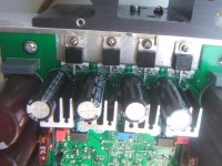
I find that since the bias for vertical mosfets is usually >150mA, allowing the system to be a bit overcompensating can buy a bit of extra stability with regard to dynamic tempco. Although the effect is small, the fets get a boost in Gm at a higher temperature.
 If the effect of overcompensation is slight, the bias can be kept within acceptable range, >100mA at maximum temperatures. Consequently, initial static bias may be a bit higher but since the devices and heatsink are cold it is of slight issue. I have had success in stablizing bias of vertical mosfets using a topology similar to the HEC Bob used, but I use small SMD devices as the error amplifiers, mounted on the PCB so as to be in contact with the drain pin close to the transistor package. Although there is a short distance of metal for the heat to traverse, it is not so effected by the time lag of the thermal insulator/heatsink. see pic from previous learning experience.
Attachments
Last edited:
I have been having a hard time putting together a bias spreader that could correctly track the 2.1mV/C NJL Vbe with the 1.7mV/C ThermoTrak diode tempco for a triple output stage that has a diamond buffer as its pre-driver and driver, which requires a bias voltage of about 1.4V. This 1.4V really is a very small play ground that doesn't house many p/n junction drops. So after some head scratching I came up with a circuit that seems to be able to serve the purpose.
The circuit diagram is in the attached pdf. It uses an op amp MAX4289 that works on as low as 1.0V supply and swings rail-to-rail. I set it up to have a gain of 2.5 to derive a 4.25mV/C for the two b-e junctions of the output transistors from the TT diode's 1.7mV/C tempco. R6 is the bias trim pot. It sets a bias current in the TT diodes so as for them to come up with a proper forward drop. R5 may serve as a supplement adjustment just in case. I could have used only one of the TT diodes to make the circuit simpler but I would feel better by using one each from the NPN and PNP devices.
I must admit I have limited experience in circuit design and engineering. Before I put it into PCB layout and make smoke in my amp I would much appreciate any of your comments and ideas about it or any other 1.4V bias spreader circuit that may track correctly with TT diodes.
By the way, Bob you wrote one awesome book! It connects many isolated "dots" and it's a pleasure to read. Thank you so much!
Hi Nattawa,
As Edmond indicated, it looks like that circuit you provided may work, and it appears quite clever. Have you SPICE'd it yet?
You are right about the bias compensation of the Diamond Buffer Triple (DBT) output stage. The good news is that the bias tempcos of the predriver and driver tend to cancel each other out. The bad news is that the only Vbes left that need the spread are those of the output transistors. As you pointed out, this does not give you a lot of voltage "room" to play with. I agree that one is wise to use one each of the P and N ThermalTrak diodes to form the bias spreader.
I do tend to like simpler more "passive" bias spreaders (less to go wrong) and there may be some other approaches that are effective. As we know, if there is a greater bias spread needed, we have more circuit flexibility in achieving the bias speader TC that we desire (see the ThermalTrack bias spreaders I showed for more conventional output stages, like Triples, in Figures 14.18 and 14.19).
One approach that I showed in the book is to use a Diamond Buffer Quad (DBQ) like I showed in Figure 25.7. This introduces a larger driver AFTER the diamond buffer, sometimes one as big as an output transistor. This is especially useful for really high power amplifiers, but is certainly practical for any power level. It now makes the bias spreader need to supply 4 Vbe and gives you more room to play and adjust tempco. The DBQ is compensated in a way like a Darlington output stage.
Another approach that can be used with the DBT to get more bias spreader headroom is to add a pair of small diodes in series with the resistor that sets the bias current of the diamond buffer. The output transistor bases are then fed from across the current-setting resistor.
One can also make a higher-voltage bias spreader and reduce its spread right at its output with a three-resistor attenuator whose inner nodes feed the bases of the DBT. The current through this resistive attenuator should be held to less than about half the total current flowing through the total spreader circuit. The necessary drops could also be obtained with diodes instead of the outer attenuator resistors. This approach does not require any additional transistors to see high voltage, as might be the case if using the DBQ.
As you know, the key to all of this is to be able to amplify the TC of the pair of TT diodes enough to achieve the needed overall TC to match the output transistor Vbes. Lots of interesting approaches are possible, and the one you showed appears to be workable and clever.
Cheers,
Bob
It uses an op amp MAX4289 that works on as low as 1.0V supply and swings rail-to-rail.
Check the datasheet, MAX4289 has only 17KHz GBW. Meaning that @17KHz there won't be any loop gain to keep the bias constant.
@ Bob, thanks again for your comments and great many ideas about the alternatives. I think I share the philosophy behind your preference of using "passive" parts where possible. My op-amp based biasing circuit is really a lazy man's quick solution.
@ Edmond, thanks for the links to the discussions about your Phoenix project. When I first saw the schematic, it reminded me of my first view of the great Milan Cathedral. It's very good that you brought up the thermal attenuation. I haven't gone that far into Bob's book to arrive at that part. I may have to consider and compensate for it in an actual design.
@ Edmond, thanks for the links to the discussions about your Phoenix project. When I first saw the schematic, it reminded me of my first view of the great Milan Cathedral. It's very good that you brought up the thermal attenuation. I haven't gone that far into Bob's book to arrive at that part. I may have to consider and compensate for it in an actual design.
Last edited:
Check the datasheet, MAX4289 has only 17KHz GBW. Meaning that @17KHz there won't be any loop gain to keep the bias constant.
Hi Waly,
I thought the bias spreader is just a floating piece of DC battery, and I thought the 17KHz GBW is way more than sufficient for any rate of temperature change over time a TT diode could ever see.... did I miss something here?
Hi Waly,
I thought the bias spreader is just a floating piece of DC battery, and I thought the 17KHz GBW is way more than sufficient for any rate of temperature change over time a TT diode could ever see.... did I miss something here?
Nope, the impedance of the bias spreader has to be low even and high frequencies, read Bob's book. You can always add a cap across the spreader, but that cap comes with other penalties in terms of distortions.
- Home
- Amplifiers
- Solid State
- Bob Cordell's Power amplifier book