Why an electrolytic and not a film cap?
Hi Telstar,
The impedance of the zener diode is fairly low, so the amount of capacitance required to reduce its noise in the audio band is typically larger than what a reasonable size film capacitor would deliver. Moreover, in an application like bypassing a zener voltage reference, I don't believe that the use of an electrolytic degrades the sonics.
Cheers,
Bob
Hi Bob,
I noticed in your book that you don't use/show capacitors e.g across zener references or any other similar use. Also the current source of 2.10f is not shown with a capacitor to somewhat filter rail variations.
Are they just left out for simplified lecture or do you think this is up to the reader to decide. If the latter is the case I presume there might be reason not to use capacitors there. Is that so? Or is it rather 'more than desireable but not really a must'?
Referencing the 2.10f to Randy's drawings he uses to split the Q2 resistor in half and places a capacitor from between the resistors to the power rail.
Would there be a reason not to place them? I will not use top notch capacitors there so maybe none is better than plain standard electrolytic capacitors?
Cheers,
Olivier
Hi Olivier,
I basically left out the capacitors in the discussion to keep it simple. However, I should have devoted some space to the need for filtering and some approaches to doing that.
Cheers,
Bob
Hi Olivier,
I basically left out the capacitors in the discussion to keep it simple. However, I should have devoted some space to the need for filtering and some approaches to doing that.
Cheers,
Bob
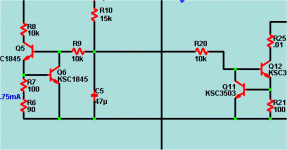
Added filtering does have it's benefits and drawbacks. With the book example ("bobamp", fig. 3.8) , adding nothing will work and there will be no turn-on thump. If you add 10uF to 47uF as C5 (below), PSRR will increase 6-8db at the input pair and just a "hair" at the OP. 10uF makes for almost NO thump , it is even hard to see on the CRO. The worst case scenario is like the fig. 3.8 amp , with it's 2 separate CCS's , individually decoupled. One or both will stabilize independent of each other or the OPS , giving a "tick" or "thump" at turn-on. (I had this "problem"
 )
)OS
Attachments
I've started the book from class D section.
Bob, you could have done better here really, there are already tons of similar popular crash courses everywhere.
You still have my need admiration of your contribution to linear amplifiers.
Hi darkfenriz,
I'm sorry that you are disappointed in the class D section in my book. It's a little hard to tell from your message if you have read all four chapters or have just started the first chapter.
You're definitely right: I could have done a better job if I had the space and that was a bigger priority for the book. I'll probably expand it in the second edition. I did say in the introduction to the class D section that I was just scratching the surface, and that is really true. The class D section is not as comprehensive as the rest of the book. Bear in mind that many readers of my book do not have a great deal of experience and knowledge with class D, so that material must start out at a fairly basic level.
You're also right about there being a great deal of information on class D out there on the net. However, it was my experience in researching the chapters that the information is spread out all over the place and very fragmented. One of the jobs of an author is to gather information on a subject and weave it into a coherent presentation, not necessarily to generate new material.
Class D is a complex and different technology. A comprehensive treatment of it would itself take a 600-page book.
You can help me in a couple of ways. First and foremost, if I have gotten anything wrong, please let me know so that I can correct it.
Second, please let me know what material you would like to see added in the second edition.
Finally, if there is a single internet site out there, or a single book out there on class D that covers the whole subject better, please let me know so that I can review it and add it to my references in my second edition.
Thank you for the feedback.
Cheers,
Bob
Added filtering does have it's benefits and drawbacks. With the book example ("bobamp", fig. 3.8) , adding nothing will work and there will be no turn-on thump. If you add 10uF to 47uF as C5 (below), PSRR will increase 6-8db at the input pair and just a "hair" at the OP. 10uF makes for almost NO thump , it is even hard to see on the CRO. The worst case scenario is like the fig. 3.8 amp , with it's 2 separate CCS's , individually decoupled. One or both will stabilize independent of each other or the OPS , giving a "tick" or "thump" at turn-on. (I had this "problem"
OS
Hi OS,
This is a really good point about decoupling and turn-on thump. Most of us have experienced annoying turn-on thump in some designs, sometimes resorting to/relying on a delayed turn-on speaker relay to kill it. Thanks.
Cheers,
Bob
Phase Margin & Gain Margin
Hi Bob,
I am a bit confused with what I measure in my simulations.
According to the setup in your book on p88 figure 4.7 you place a large inductor to make it possible to break the loop in order to measure the gain & phase margin of the loop itself (I hope to be right till here)... I added the AC analyses of this method in this reply under AC Analysis2.pdf
It is clearly visible that the GM=28dB and the PM=90°
If I do the AC analyses with the amplifier schematic back to normal (removed inductor, input signal back to the input side,...) still measured on the output and still without any input LP filter (shunt capacitor) the results show me an unstable amplifier because PM and GM are totaly inadequate. See AC Analyses1.pdf ...
If this is important, there is no OPS yet implemented in schematic.
I must be missing something. Could you tell me a bit more about how I should interpretate my results compared to your book instructions? Is this amp stable or not?
Thanks in Advance
Olivier
Attachments
Hello Oliver,
From first measurement, amplifier seems ok.
Second measurements shows input/output transfert function? ok. So how do you conclude something is unstable? No peaking in response, that seems ok.
What I read is that this amplifier have a nice 200k-300kHz bandwidth (-3dB). Phase is smoothly moving above 10kHz up to 180° at 7MHz.
Hi Bob,
I am a bit confused with what I measure in my simulations.
According to the setup in your book on p88 figure 4.7 you place a large inductor to make it possible to break the loop in order to measure the gain & phase margin of the loop itself (I hope to be right till here)... I added the AC analyses of this method in this reply under AC Analysis2.pdf
It is clearly visible that the GM=28dB and the PM=90°
If I do the AC analyses with the amplifier schematic back to normal (removed inductor, input signal back to the input side,...) still measured on the output and still without any input LP filter (shunt capacitor) the results show me an unstable amplifier because PM and GM are totaly inadequate. See AC Analyses1.pdf ...
If this is important, there is no OPS yet implemented in schematic.
I must be missing something. Could you tell me a bit more about how I should interpretate my results compared to your book instructions? Is this amp stable or not?
Thanks in Advance
Olivier
Hi Olivier,
I'm sorry that I've been tardy in getting back to you. Macleod's comments are right. The amp is fine. The only thing I see (which I may be misinterpreting) is that the closed loop gain on your graph looks to be about 36 dB, where I believe the expected gain for the amplifier arrangement of that figure should be 26 dB.
The thing to bear in mind is that you should not be trying to measure phase and gain margin from the closed loop gain curve.
Cheers,
Bob
Gain & Phase Margin
Hi Bob, Hi Macleod,
I understood that CL phase and gain measurement are pretty useless. So even if the CL gain goes throug zero at 10MHz and the phase at that point is already way beyond 180° lagging, that is not a direct concern... right?
Indeed measuring openloop (while breaking the loop with a large inductor) the result seem promising. If this figure defines the PM and GM I am happy.
FYI, for now, the compensation capacitor over the VAS is a simple miller cap, however stretching over a darlington and cascoded vas...
Bob, according to me the 36dB is normal. Where do you deduct from that the gain should be 26dB?
I will now try to incorporate TMC where I follow Edmonds view. But anyway according to your book and the many forum topics here the TMC camp seems to be more convincing than the TPC camp. My main reason is that I don't like the peaking in the bode plot...
Olivier
Hi Olivier,
The closed loop gain for the amplifier in my book should be 20, since the feedback network consists of a 19k and a 1k resistor, which results in a 20:1 attenuation in the feedback path. A voltage ratio of 20:1 corresponds to 26 dB. That's why I'm not sure how you got 36 dB.
I agree that TMC is preferable to TPC, at least in my opinion. However, the TMC vs TPC discussion that we had here brought more understanding to the problem, particularly in regard to analysis for stability.
Cheers,
Bob
PM & GM
Hi Bob,
OK I see what you mean. In my circuit the feedback resistors are set at 15K and 270R and therefore the midband gain is around 36dB.
About compensation... I didn't go through all of the book yet but I read and saw several times on the net that placing a resistor in series with the compensation capacitor includes a zero in the bodeplot.
In TPC and TMC it is possible to insert 2 resistors in one would like... but what could be the gain of this? Which side to put it? Both sides?
Cheers,
Olivier
Hi Olivier,
Great question about compensation. In most of my designs, I have made provision for a resistor in series with the Miller compensation capacitor. This includes the Miller input compensation scheme that I used in my MOSFET power amplifier with error correction. You are correct - that resistor adds a zero in the forward path by "stopping" the continuation of the 6 dB/octave rolloff of the Miller compensation. This zero must be used judiciously or it will cause a loss of gain margin. The zero is usually placed well above the gain crossover frequency.
Although I have not used it with TMC, I know of no reason why it cannot be carefully applied to a TMC compensation scheme. Without having given it much thought, I would add the resistor between C1 of the TMC network and the input base of the VAS.
Cheers,
Bob
VAS Current limiter
Hi Bob,
I incorporated the classic VAS Iq limiter. The base-emitter of the protection Q stands across the VAS Q (not the cascode Q but the amplifying Q). The collector of the protection Q goes back to the base of the beta enhancer Q. Nothing special here.
However I would like to have a led lighting up when the circuit goes into protection. How can this be done? It should not interfere with the signal nor with the protection function itself and it should be quite binary, I mean led on when protection is on and vice versa ... Reducing in betweens as much as possible ...
cheers,
Olivier
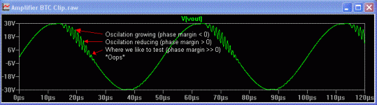
Hi BobThe stability of power amplifiers can be rather different in different operating regions...
I can't tell you how many times I've seen amplifiers break out into a burst of oscillation on the falling slope at high amplitude of a sinewave just under clipping...
You gave a perfect example of this back here:
I was surprised by how bad the ringing was with TPC and decided to do a little investigation. My starting assumption was that reduced phase margin will increase the tendency to ring, but that you still have to kick a thing to make it ring. E.g. Rail sticking during clipping will give the circuit a nice kick when it "unsticks", and could initiate nasty ringing.I've done some more simulations on CMC, TPC and TMC and have attached a zipped folder of three simulations ...
It is easy to see that both TPC and TMC do not recover from clipping as well as CMC. However, TPC is much worse than TMC...
So my first step was to modify the VAS to get inherently clean, fast, symmetrical clipping. This resulted in a big improvement, but there was still visible ringing, and it was still much worse on the positive half.
That made me curious about whether the phase margin was varying with output level, so I tried a quick test with a staircase waveform. The first run showed the ringing getting slightly worse at higher levels, but about the same on both sides. Increasing the output level a bit revealed the problem, though.
When the NPN output device is conducting more than about 5.5A, the amp is totally unstable. Testing with various loads and output levels seemed to confirm that. Adding an extra pair of output devices fixed the problem (although it would probably still have problems above 10A, I didn't bother testing further.)
This was quite an eye-opener for me. I have thought it a good idea to operate output devices "below the knee" for other reasons (e.g. distortion), but it never occurred to me before that it might be important for stability too. It also served as a gentle reminder that checking bode plots under quiescent conditions doesn't even begin to tell the whole story.
Cheers - Godfrey
Attachments
Hi Bob,
I incorporated the classic VAS Iq limiter. The base-emitter of the protection Q stands across the VAS Q (not the cascode Q but the amplifying Q). The collector of the protection Q goes back to the base of the beta enhancer Q. Nothing special here.
However I would like to have a led lighting up when the circuit goes into protection. How can this be done? It should not interfere with the signal nor with the protection function itself and it should be quite binary, I mean led on when protection is on and vice versa ... Reducing in betweens as much as possible ...
cheers,
Olivier
Hi Olivier,
If I understand you correctly, you are talking in the context of a single-ended VAS that is loaded with a current source (correct me if I am wrong, and what I say might apply to certain complementary VAS stages anyway). If you are in te context of the single-ended VAS, the LED will only light when the amplifier is clipping in one direction (trying to turn the VAS Q on too hard).
The challenge in illuminating an LED when this classic VAS current limiting scheme is used is that it appears you have only one Vbe plus the VAS emitter resistor drop to work with when the circuit is protecting. One approach might be to use a matched differential pair of transistors for the protection transistor and make it part of a current duplicator, where the added transistor is arranged to conduct approximately the same current as the protection transistor. Maybe put a little bit of degeneration in each emitter of the pair, but no so much that it interferes with the protection action. Also, you might want each of the pair of transistors to have their base go the the VAS emitter through a 100 ohm resistor to make life safe for each of the pair of transistors and to prevent the added transistor from dragging down the base of the protection transistor if the added transistor saturates. Use the current flowing in the collector of the added transistor to light the LED. Just thinking out loud here.
Cheers,
Bob
Led VAS protection
Hi Bob,
I am using a complementary IPS & VAS. On one side I think it's too much components and too much potential interference to have just an led indication but on the other hand, the used amplifier topology is very complex so it doesn't come to one or two more components... I am unsure what to do for now.
But I choose not to go that road for now, the led can come in later when the circuit proto works in reality.
As you know I have to tame the fighting VAS Iq. I use a CMCL for it which seems to work well in simulation and also in reality for some part (that is in my circuit). My major problem for now is that my phase lag grows faster than it should with rising frequency.
I will redesign my pcb because I hope it suffers PCB layout problems such as : parasitic capacitors. One that bothers me much is the node between the IPS output and VAS input (on both sides). All summed this track is very long because it connects many components : Q mirror, Q diff, IPS clamp diode, VAS input Q, RC filter to rail, CMCL Q, protection Q, VAS clamp diode, compensation circuit.
Not only the length of the track is an issue but its impedance value must probably play a role as well as the amount of connections it has...
Do you think my trouble could have its origin on the pcb? Or is its impact usualy soo small I should search elsewere....
Is there a particular point to keep in mind?
Cheers,
Olivier
Wow! It seems so obvious now you point it out!AC analysis is by definition carried out at infinitesimal AC level. To vary operating point add DC voltage sources in the feedback path (shifts output voltage) or DC current sources from the output to ground (shifts output current).
Samuel
thank you for the tips, I will now step a param for output voltage to check that!
- Home
- Amplifiers
- Solid State
- Bob Cordell's Power amplifier book