It’s not often you see a quad diamond.
Have you ever seen a quad diamond before Bogdan?
As Bob says there are no problems with a “quad” diamond if you follow the “normal” guidelines that Bob mentions.
BTW the BIAS circuit that Bob are using with the quad is depending on the standing current in the VAS. Wouldn’t it be better to make the BIAS independent of the VAS current?
Cheers
Stein
Hi Stein,
Are you referring to the diamond buffer quad output stage I describe in Figure 25.7?
That output stage consists of a diamond buffer followed by a double EF output stage, so the net amount of bias spread needed is about 2 Vbe per side, or about 4 Vbe total. The quiescent bias in the output transistors in this arrangement is controlled in the usual way, typically by a Vbe multiplier-based bias spreader. As such, it is relatively independent of the VAS standing current.
The diamond buffer provides the pre-driver and pre-pre-driver functionality.
Perhaps I am missing your point in some way or you are referring to a different circuit.
Cheers,
Bob
Bob if OPS is on separate PCB, is it better to separate LPF`s grounds from the zobel ground and connect each of them to the power supply`s main star ground through separate wires?
Hi bogdan,
I would connect all of the OPS bypass capacitors and the Zobel to the same output stage ground, with that ground going back to the star ground.
Cheers,
Bob
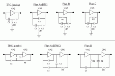
Hi BobSome of you may recall that I introduced what I called Bridged-T Compensation (BTC) in Chapter 9 of my book, figures 9.4 and 9.5. It is TPC with a small capacitor bridging the "T", connecting directly from the VAS output to the VAS input. This capacitor that I will call C3 here is no more than a couple of pF. It eliminates the very large peak that we have seen here in the TPC loop gain characteristic...
The same result can be achieved by adding an extra resistor (R2) in parallel with one of the capacitors. (See first row of pics below).
With TMC, I suspect the peak can also be removed by adding a resistor, this time in parallel with C2. (See second row of pics below).We have also seen here that if one examines the total loop gain seen by the output stage in a TMC design, we also see pretty much the same peak. Placing a small bridging capacitor across the TMC network in the same fashion as BTC yields the same benefit in what we might now call bridged TMC (BTMC).
In each of these cases, the value of the resistor should be about equal to the reactance of the capacitor it is connected across, at the frequency of the peak. For a more rounded corner in the plot, the resistor could be reduced to perhaps half that value.
I thought these alternatives worth mentioning as it may be more practical (or convenient) to add an extra resistor, rather than an extra capacitor.
Cheers - Godfrey
p.s. Sorry this is a few days late
Attachments
Hi Bob
The same result can be achieved by adding an extra resistor (R2) in parallel with one of the capacitors. (See first row of pics below).
With TMC, I suspect the peak can also be removed by adding a resistor, this time in parallel with C2. (See second row of pics below).
In each of these cases, the value of the resistor should be about equal to the reactance of the capacitor it is connected across, at the frequency of the peak. For a more rounded corner in the plot, the resistor could be reduced to perhaps half that value.
I thought these alternatives worth mentioning as it may be more practical (or convenient) to add an extra resistor, rather than an extra capacitor.
Cheers - Godfrey
p.s. Sorry this is a few days late
Hi Godfrey,
Great post and nice diagrams to illustrate. If it works as well in all regards it is certainly preferable to add a resistor instead, since small-value capacitors, like 0.5 pF to 2 pF, are not always as easy to obtain, and cost more.
Cheers,
Bob
if you have "diamond" shapes then you should use them for the gm of the "VAS" - Mike's quite right that "TIS" for transimpedance stage is more appropriate (but the name change is not going to happen at this late date)
using a gm specific symbol keeps the gain limitations with loading more in the forefront in contrast to the expectation of relative load independence with a (implied) Vgain - "VAS" Volatge gain is 1st order determined by load Z
using a gm specific symbol keeps the gain limitations with loading more in the forefront in contrast to the expectation of relative load independence with a (implied) Vgain - "VAS" Volatge gain is 1st order determined by load Z
Last edited:
by andrew T . - yes, the different LTP current would require a different emitter resistor value for the same degeneration.
Bob quotes this 10x degeneration quite a lot.
Hi Andrew,
We usually don't think in terms of degeneration in drivers and output stages. I like 10:1 because it linearizes the stages very significantly and usually has little impact on the noise of the amplifier. Some are concerned about the effect of increased amplifier noise with such amount of degeneration in the LTP, but overall amp simulations often show that this does not seriously degrade the noise in such an application. Power amplifier input-referred noise less than about 10 nV/rt Hz is more than adequate.
Cheers,
Bob
I tried widely varying LTP currents both on the real amp and in my LT. In the simulation I saw little change (below 1) in the CLG even as I .step'ed my tails between .6 mA and 2.2mA. On the real amp , sonically ..there was a "sweet spot" where the sound was "best" (subjective but tangible) at 1.7ma.
Changing the actual LTP re's has a major impact both in the LT/real world , I made a mistake and used 10R instead of 100R .. WHOA! SMOKED A ZOBLE (oscillation). By backing off on the CCS current , I could even stop the oscillation before realizing my "old man" eyes confused black for brown.

OS
Attachments
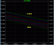
I tried widely varying LTP currents both on the real amp and in my LT. In the simulation I saw little change (below 1) in the CLG even as I .step'ed my tails between .6 mA and 2.2mA. On the real amp , sonically ..there was a "sweet spot" where the sound was "best" (subjective but tangible) at 1.7ma.
Changing the actual LTP re's has a major impact both in the LT/real world , I made a mistake and used 10R instead of 100R .. WHOA! SMOKED A ZOBLE (oscillation). By backing off on the CCS current , I could even stop the oscillation before realizing my "old man" eyes confused black for brown.
OS
Hi OS,
Your results appear to be pretty much as expected. When the LTP is substantially degenerated, changes in the external emitter resistance will far outweigh changes in the tail current (which change the smaller re).
As you know, I like 10:1 emitter degeneration, but others may prefer less. The 10:1 emitter degeneration is best when a Darlington VAS is used and the LTP is loaded with a current mirror. Designs that use a resistor to load the LTP and only a single-transistor VAS may not be able to afford the loss in IPS gm due to significant amounts of degeneration.
I also like to degenerate the VAS by 10:1 or more.
Cheers,
Bob
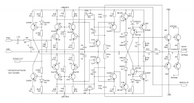
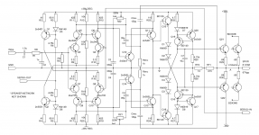
Bob, please take a look at this thing
Hi Bob, I always follow your posts with great attention and respect.
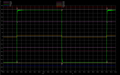
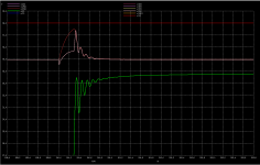
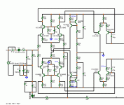
I would like you to comment my design that introduces (I believe as didn't see this technique before) a special VAS, that allows very very low degeneration at LTP inputs. Take a look at R12, C5 appears to be a conventional RC low pass filter, but it is more than that it seems, as there is a strong coupling (nonlinear) through the emitters of diff. VAS Q12, Q11. I have reasonably speculated that as each leg has it own and different natural frequency (of oscillation), s1 and s2 the pair acts as a 'mixer' absorbing energy at expenses of the 'oscillator leg' (could be one or another) and spreading apart as s1+s2, s1-s2 outside the 'resonance frequency' of each other. To empathize this mechanism (i have extensively simmed, including the parasitics {as much I could}), the first pix (extreme0) show the response of the amp with 0 degeneration for 'torture' square wave input (yellow) and the output (green) ringing for a short period. The second pix (extreme1) shows the detail of the transient at one input at the VAS (red,pink) and the output (green) with 1 OHM degeneration at LTP inputs, see the rapid collapsing of oscillation.
Don't pay much attention at the selection of components because is what I have on hand in Chile.
The numbers for a 2.2 OHM degeneration are:
215 V/usec slew leading edge, 245 V/usec trailing edge.
THD's at full power ~70 Watts: 5.5 ppm @ 10KHZ, 44ppm @ 100KHZ, 160ppm @ 400KHZ, at 31 Watts output 1.9 ppm @ 10KHZ, 9.7ppm @ 100KHZ, 50ppm @ 400KHZ
So I've decided to build it, (a great bet !!!) as I am confident that I will have lots of room to make it stable with a very decent performance.
I would be very grateful to receive your comments,
(I will tell you the outcome of this adventure, so maybe if I succeed you can include it in your next book ... a little bit of humour ...)
Cheers
Arturo
Hi Bob, I always follow your posts with great attention and respect.
I would like you to comment my design that introduces (I believe as didn't see this technique before) a special VAS, that allows very very low degeneration at LTP inputs. Take a look at R12, C5 appears to be a conventional RC low pass filter, but it is more than that it seems, as there is a strong coupling (nonlinear) through the emitters of diff. VAS Q12, Q11. I have reasonably speculated that as each leg has it own and different natural frequency (of oscillation), s1 and s2 the pair acts as a 'mixer' absorbing energy at expenses of the 'oscillator leg' (could be one or another) and spreading apart as s1+s2, s1-s2 outside the 'resonance frequency' of each other. To empathize this mechanism (i have extensively simmed, including the parasitics {as much I could}), the first pix (extreme0) show the response of the amp with 0 degeneration for 'torture' square wave input (yellow) and the output (green) ringing for a short period. The second pix (extreme1) shows the detail of the transient at one input at the VAS (red,pink) and the output (green) with 1 OHM degeneration at LTP inputs, see the rapid collapsing of oscillation.
Don't pay much attention at the selection of components because is what I have on hand in Chile.
The numbers for a 2.2 OHM degeneration are:
215 V/usec slew leading edge, 245 V/usec trailing edge.
THD's at full power ~70 Watts: 5.5 ppm @ 10KHZ, 44ppm @ 100KHZ, 160ppm @ 400KHZ, at 31 Watts output 1.9 ppm @ 10KHZ, 9.7ppm @ 100KHZ, 50ppm @ 400KHZ
So I've decided to build it, (a great bet !!!) as I am confident that I will have lots of room to make it stable with a very decent performance.
I would be very grateful to receive your comments,
(I will tell you the outcome of this adventure, so maybe if I succeed you can include it in your next book ... a little bit of humour ...)
Cheers
Arturo
Attachments
Hi Bob, I always follow your posts with great attention and respect.
I would like you to comment my design that introduces (I believe as didn't see this technique before) a special VAS, that allows very very low degeneration at LTP inputs. Take a look at R12, C5 appears to be a conventional RC low pass filter, but it is more than that it seems, as there is a strong coupling (nonlinear) through the emitters of diff. VAS Q12, Q11. I have reasonably speculated that as each leg has it own and different natural frequency (of oscillation), s1 and s2 the pair acts as a 'mixer' absorbing energy at expenses of the 'oscillator leg' (could be one or another) and spreading apart as s1+s2, s1-s2 outside the 'resonance frequency' of each other. To empathize this mechanism (i have extensively simmed, including the parasitics {as much I could}), the first pix (extreme0) show the response of the amp with 0 degeneration for 'torture' square wave input (yellow) and the output (green) ringing for a short period. The second pix (extreme1) shows the detail of the transient at one input at the VAS (red,pink) and the output (green) with 1 OHM degeneration at LTP inputs, see the rapid collapsing of oscillation.
Don't pay much attention at the selection of components because is what I have on hand in Chile.
The numbers for a 2.2 OHM degeneration are:
215 V/usec slew leading edge, 245 V/usec trailing edge.
THD's at full power ~70 Watts: 5.5 ppm @ 10KHZ, 44ppm @ 100KHZ, 160ppm @ 400KHZ, at 31 Watts output 1.9 ppm @ 10KHZ, 9.7ppm @ 100KHZ, 50ppm @ 400KHZ
So I've decided to build it, (a great bet !!!) as I am confident that I will have lots of room to make it stable with a very decent performance.
I would be very grateful to receive your comments,
(I will tell you the outcome of this adventure, so maybe if I succeed you can include it in your next book ... a little bit of humour ...)
Cheers
Arturo
Hi Arturo,
I've looked at your amplifier circuit and have trouble understanding its operation in terms of it being able to have virtually no degeneration of the LTP, have such high slew rate, and be stable. The waveforms appear to exhibit instability. I'm just not sure how the magic works. What is the gain crossover frequency, phase margin and gain margin?
What is your objevtive in seeking very low degeneration of the IPS?
How is the output stage quiescent bias set?
The RE values of 0.68 ohm seem rather high.
You mention Ctmc, suggesting that you are using TMC, but what you have looks like TPC.
Best of luck,
Bob
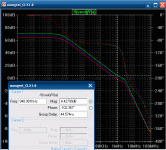
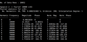
I had a hard time understanding artu's amp at first , but realized it was similar to Dave tilbrook's AES6000. I degenerated it more conservatively , actually "grafting it" onto my leach prototype simulation. I was impressed by the clipping , transient ,and general robust behavior of the circuit. (Below 1) is the Bode for 60,40, and 20R degeneration - green trace. 47R was what I settled for , giving me 900k UG and 78db margin. This gave me about half of what Artu achieved, 125/Vus PERFECT symmetric slew along with stellar ... almost "soft clipping" behavior. I also have almost achieved PPM levels , but that is not my greatest concern. The FFT's are nice , too (2nd dominant - high order very low) .. this amp should sound VERY good. My "take" on it is (below 2 - CLX). I most likely will just drive a pair of laterals or my EF2 with it.
OS
Attachments
Last edited:
I'm confused by the diodes marked "1N5918". I thought 1N5918 is a 5.1V zener. If these are normal diodes, then it looks like the output stage operates in class A with about 1 amp of idling current through each output device. Is this correct?
Hi Samuel,
The 1N5918 is indeed a 1.5W 5.1V Zener diode, but it is used in the schematic as a forward-biased conventional diode, so I am confused as well. I'm not that familiar with the "forward" characteristics of a Zener diode, but maybe those characteristics differ in a way that was advantageous for this application.
Cheers,
Bob
Bob, thank you very much for your time, analysing my amp
Hi Bob,
With the 3.3 OHM degeneration and the C5, C6 'dumpers', the phase margin is about 96° (f=4 MHZ). My goal was to stress as much as possible before reaching instability. If you strip C5,C6 caps the amp becomes unstable, no doubt, so in that case the need of a conventional degeneration is mandatory, and maybe also including the VAS degeneration as OS did in CLX. So why such little degeneration? because in part reduces distortion, but mainly it enhances the harmonic content distribution (empirically found), at a very high audio BW (exceeding 100KHZ), OS confirmed same results. The clipping is not as clean as OS CLX, but stable up to MHZ's. Anyway at first live tests I will start at much higher degeneration, and verify how much I can decrease it, and when reaching the final values I will test it with a 4GB HP spectrum analyser (with a friend that works at a telecom company), to see how much 'good' this thing is. The .68R are for stabilize the OPT darlingtons (4 totems which are very hard drived by the 0.8 OHM output impedance buffer) as much as possible to prevent thermal runaway (despite the thermal coupling), each one will be loaded with a current bias of 675 ma, so the total quiescent current wil be ~ 2.7 Amps. (Class A, at 100KZ a little bit AB). Yes you are correct the feedback network is TPC (a typo inherited from the previous schematic). As I said, I will have lots of room for experimentation, to tune the final values, and achieve as OS said a very good precise sound (I hope !!!)
Thank you very much for your attention Bob,
Cheers.
Arturo
Attachments
Hi Godfrey,
the 1N5918 are schottky diodes, and has different thermal profile than conventional normal (minority carriers) diodes and less voltage drop. So when the temperature raises and the output stage gets hotter, the quiescent current drops, keeping the darlingtons within the SOA curve. Their purpose is thermal compensation.
the 1N5918 are schottky diodes, and has different thermal profile than conventional normal (minority carriers) diodes and less voltage drop. So when the temperature raises and the output stage gets hotter, the quiescent current drops, keeping the darlingtons within the SOA curve. Their purpose is thermal compensation.
The corrected schematic (it is a transcript, because the simulations are done with 'text mode' ngspice, I don't know if exists a GUI front end for ngspice or spice3).
Hi, Artu
Out of curiosity, i did some sims of your amp , and it appears
that as published in Ostripper s thread, it s instable.
As i already pointed it , degeneration is clearly too weak,
and the value must be increased to about 22R.
Also,current is very high, and the relevant bjts are undersized
if reliabilty is a concern.,
The amp has irregular step response, with the slope abruptly changing
at half course, the cause of wich i didn t still check about.
The output darlingtons , although with a 20mhz ft are somewhat
not very adequate, unless you parallel three pairs.
Hope that you ll find easy fix for those points.
Cheers,
w
Out of curiosity, i did some sims of your amp , and it appears
that as published in Ostripper s thread, it s instable.
As i already pointed it , degeneration is clearly too weak,
and the value must be increased to about 22R.
Also,current is very high, and the relevant bjts are undersized
if reliabilty is a concern.,
The amp has irregular step response, with the slope abruptly changing
at half course, the cause of wich i didn t still check about.
The output darlingtons , although with a 20mhz ft are somewhat
not very adequate, unless you parallel three pairs.
Hope that you ll find easy fix for those points.
Hi Wahab,
Can you elaborate a little bit more specific?, about stability, did you find an oscillation condition? or is overshoot or transient recovery? and the 'irregular step response' of the slope (I didn't noticed yet), the current issue is about, input VAS or the buffer?
Maybe the schem isn't enough clear, but the output stage has four pairs in parallel (4 totems).
I will review again the schem, please refer to the circuit above, the original had some typos (the schottky diodes NOT ZENERS).
Cheers
Arturo
- Home
- Amplifiers
- Solid State
- Bob Cordell's Power amplifier book