Hi Bob and others,
I went through the old book, looking for answers about matching transistors for the o/p stage. Found some information, but maybe you can elaborate.
There is some discussion in another thread about matching bjts in a OPS
Matched output transistors: does gain change with age?
Chris was referencing the OnSemi datasheet (MJ21193, MJ21194) where they showed the test of measuring open loop thd in a pair of devices, matched and un-matched.
How much matching needs to be done and how?
Got to wondering if you're matching OPS devices, make any sense to select/match the ballast(emitter) resistors too?
Thinking that the processes are so fine tuned now it might be difficult to find matches if there is no overlap in hfe?
I see ECW20N20-S - Selected Lateral Mosfet selling matched pairs of lateral fets
Good question, Rick. The relative need for matching output transistors and its effect on distortion and thermal stability depends a lot on the details of the output stage. First of all, there are the two issues of Vbe matching and beta matching. There is also the same issue with regard to paralleled pairs of the same sex and pairs of opposite sex.
For output stages with Triples (e.g., 3EF), there is plenty of net current gain, and beta doesn't matter as much, even when there is some beta droop. This is one reason I like Triples; they greatly reduce the need for beta matching, either same-sex or opposite sex. The tiny extra cost of pre-drivers is somewhat canceled by the reduced need (maybe zero) to match betas.
However, thermal stability and current-hogging must also be considered. If your output stage has large base stopper resistors (e.g., more than 4.7 ohms) and small emitter resistors (e.g., less than 0.22 ohms) there can be some current hogging among some same-sex paralleled devices, since beta differences may cause some small differences in voltage drop across the base stopper resistors, resulting in different bias current for a given Vbe. As the higher-beta device draws more current and gets hotter, its beta goes up more and its Vbe goes down, both reinforcing the difference in current draw. I virtually always use 2.2 ohm base stoppers and 0.22 ohm emitter resistors.
I do not try to match NPN-PNP beta or Vbe. For same-sex paralleled devices, I just use devices all out of the same tube.
Cheers,
Bob
I virtually always use 2.2 ohm base stoppers and 0.22 ohm emitter resistors.
Hi Bob - Does this heuristic apply to single pair output stages or just output stages with multiple pairs of paralleled devices? Is it EF specific or CFP output stages as well?
Thanks
Well, I've pre-ordered the 2nd Ed. and cannot wait for it to land.
Thank-you, @Bob Cordell, for the effort involved and - no less a thing- your continued good-humoured and detailed responses to the thoughts, queries & discussion here. Though I hope you already realise the flood may not, actually, abate after a brief pause, just because the 2nd ed. lands on our doormats soon ...")
With thanks,
Martin
Thank-you, @Bob Cordell, for the effort involved and - no less a thing- your continued good-humoured and detailed responses to the thoughts, queries & discussion here. Though I hope you already realise the flood may not, actually, abate after a brief pause, just because the 2nd ed. lands on our doormats soon ...
With thanks,
Martin


Hi Bob and other forum members.
When you have time I'd be interested to hear you opinion on the grounding layouts. One is from your book and one is from another thread here on DIY. View attachment 749428 View attachment 749429
The most important on board grounding is to return the signal ground to the load and then to the local star ground. Returning the signal and load ground's separately to any other locations will cause a error voltage to develop which will lead to increased noise and worse THD measurements. All PCB designs from proven high precision designs follow this formula. For example have a look at the attached PCB from a low distortion design, you can see the signal ground from the left joining the speaker (load) ground from the right before then joining the local star ground in the middle at the bottom layer of the board.
Low Distortion PCB design is a black art involving proper grounding, decoupling, stray capacitance/inductance considerations, loop area reductions (note in the attached PCB how the V+ and V- traces are right next to each other) considerations etc and i am unable to find any book which tackles this subject. I wish Bob would consider adding a chapter on low distortion PCB design for amplifiers in his next book, if he has not already done so.

Last edited:
Hi Bob - Does this heuristic apply to single pair output stages or just output stages with multiple pairs of paralleled devices? Is it EF specific or CFP output stages as well?
Thanks
I use these values virtually all of the time. However, the use of base stopper resistors is less needed for single-pair output stages. I must admit, I have not done a single-pair output stage in a very long time. The use of 2.2 ohm base stoppers would also apply to multi-pair CFP output stages. For CFP output stages, the value of the resistor corresponding to the output emitter resistor is a little less obvious, and it is notable that Self often uses 0.1 ohm.
Cheers,
Bob
Well, I've pre-ordered the 2nd Ed. and cannot wait for it to land.
Thank-you, @Bob Cordell, for the effort involved and - no less a thing- your continued good-humoured and detailed responses to the thoughts, queries & discussion here. Though I hope you already realise the flood may not, actually, abate after a brief pause, just because the 2nd ed. lands on our doormats soon ...
With thanks,
Martin
Thanks Martin!
Cheers,
Bob
Hi Bob and other forum members.
When you have time I'd be interested to hear you opinion on the grounding layouts. One is from your book and one is from another thread here on DIY. View attachment 749428 View attachment 749429
Hi Stuart,
That illustration from my book is a bit over-simplified, depicting what one might call a traditional star ground in a figure whose main purpose is to illustrate the use of a split reservoir capacitor. In reality, I usually don't use an idealized star ground like that. It tend to use an arrangement more like a star-on-star ground.
The most important guiding principle, in my view, is to follow the currents, recognizing that every ground wire or trace has some impedance. One can also use the fact that current tends to follow the lowest-impedance path to advantage, directing currents to flow in the directions that you want them to, and through the paths that you want them to.
I also don't like to have high ripple currents flowing through a star ground for which other parts of circuits rely on as ground, recognizing that a physical single star ground can really only be truly equipotential in an ideal world. For example, I merge the common of the reservoir capacitors and the transformer center tap together at a single point and then route that ground point to what might be considered a single point ground. This keeps the heavy ripple currents from flowing through the single point ground node. The split reservoir capacitor approach helps in this regard, and the small-value resistors between the first and second sets of reservoir capacitors help keep the heavy ripple currents flowing in the paths desired.
The fact that the amplifier board is physically different and apart from the main power supply also influences the choice of grounding architecture. On the power amplifier board, there is the essence of a modified star ground. On the board, I will virtually always bypass the main rails locally with 1000 uF capacitors. I usually join the common (ground) ends of these capacitors together and then route that node to what I will call the equivalent of the amplifier board star ground. This again keeps ripple current that flows through those capacitors from flowing through the local star ground. This also helps to resolve the positive and negative rail half-wave rectified signal currents into a sinusoid before being connected to the local star ground.
At this board star ground, the ground from the power supply, the ground from the 1000 uF rail capacitors, the ground from the loudspeaker, and the ground from the rest of the amplifier are tied together. A significant choice that I make is to not route the loudspeaker neutral line back to the power supply star ground; I always return the speaker current to the amplifier board.
Cheers,
Bob
Bob I've questioned whether the board power rail bypass capacitors should be returned on a separate ground to the main reservoir. What's you take on this.
I always return the board rail capacitors, like the 1000uF local rail bypass/reservoir capacitors, to the local ground on the board. As mentioned earlier, I connect their commons together, then return that to the local ground node on the amplifier board. This is the node where incoming power supply ground, speaker return, and the rest of the ground meets. It is pretty much a star ground on the amplifier board. From that ground back toward the input end of the board, I have what could be called a tree ground structure. This is like a ground line that travels across the center of the board, to which other grounds along the way connect. Relatively little power supply rail bypass current and signal current flow in this ground line.
If a ground plane is being used, this is where it would connect. A ground plane is not usually necessary, but if one is used, bear in mind that it is not necessarily equipotential if currents are flowing in and out of it. With a ground plane, you actually lose some control of where and how such currents flow.
I also use what I call progressive rail decoupling. The output transistors are fed from the rails that are locally bypassed with the 1000 uF capacitors from the rail voltages from the power supply. An R-C filter consisting of an ohm or two and 100+ uf to ground then feeds further filtered rail to the driver collectors. From there, a second R-C filter consisting of 10-20 ohms and 100+ uf feeds still further filtered rail voltages to the predrivers, VAS and IPS. This really cleans up the rails, especially at higher frequencies. It also effectively blocks high-frequency signal voltages induced onto the rails from making its way back to earlier stages, suppressing the possibility of HF oscillations.
Finally, the low impedances of these R-C filters, and the fact that they look like Zobel networks to the feeding node, damp HF resonances on the rails, further contributing to stability at high frequencies. Those series resistances also reduce the likelihood of those additional bypass capacitors dumping garbage current into the ground as it progresses back toward the input stage of the amplifier.
For stability, I generally put a zobel network shunt from the output of the VAS to ground. This network is usually about 100 pF and 100 ohms in series. It helps guarantee that that node stays relatively resistive-looking regardless of what the VAS Miller compensation feedback is doing The output of a shunt feedback circuit can sometime begin to look inductive at high frequencies). Bear in mind that if the amplifier clips, that Miller shunt feedback may stop being effective in keeping that node low impedance at high frequencies. The 100 pF limits VAS slew rate to about 100 V/us for a single-ended VAS operating at 10 mA.
If using a 3T current mirror with a helper transistor, I place a 470 pF capacitor from base to emitter of the helper transistor to reduce its ft and reduce HF inetractions between the output of the current mirror and the input of the 2T VAS.
Cheers,
Bob
I second that. Thanks for such a detailed answers Bob I appreciate your time in responding with such insightful information.
I like the Idea of a specific chassis star ground point not on the PSU or Amplifier boards. I can connect my speaker protection board ground to that point too.
I was also wondering where do you run your signal ground and safety ground too.
Do you run your signal ground back to the Amplifier star ground point were the speaker return ground, the power supply ground and the chassis star ground is connected?
Then connect the safety ground to the chassis star ground point. I guess that this point could be insulated from the chassis so if a ground lift circuit is used you can create a difference in potential between the chassis star ground point and the safety ground which of course is connected directly to the chassis.
Last edited:
Comment on ground. I have been working on a preamp design (part of a vintage receiver restoration/modernization project) using LM4562 op amps. They have no actual ground connection, just the ±15 V supply. Bypass ground was run separately from signal ground back to a common ground bus. This thing was oscillating in the MHz region. After much investigation and reworking, I was finally able to duplicate the problem with a single stage on a breadboard. It would only oscillate with the op amp connected in the inverting configuration. The usual small capacitors connected in various locations at the op amp did not help. If I short the bypass ground to the signal ground at the amplifier (they are connected to exactly the same point about 6 inches away), the oscillation stops. The bypass ground appears clean, so I eventually connected the signal ground to the bypass ground at the preamp boards with a 4.7 Ω resistor. The complete preamp section is now installed, wired, and seems to be ok. But, this goes against everything we have been told about keeping the grounds separate back to a central ground point.
Scott Wurcer said to me once "If you have to do 7 board layout with different grounding so be it.".
Whatever works.
I kept remembering the quote from Thomas Edison: "I have not failed. I have only found 10,000 things that don't work."
Comment on ground. I have been working on a preamp design (part of a vintage receiver restoration/modernization project) using LM4562 op amps. They have no actual ground connection, just the ±15 V supply. Bypass ground was run separately from signal ground back to a common ground bus. This thing was oscillating in the MHz region. After much investigation and reworking, I was finally able to duplicate the problem with a single stage on a breadboard. It would only oscillate with the op amp connected in the inverting configuration. The usual small capacitors connected in various locations at the op amp did not help. If I short the bypass ground to the signal ground at the amplifier (they are connected to exactly the same point about 6 inches away), the oscillation stops. The bypass ground appears clean, so I eventually connected the signal ground to the bypass ground at the preamp boards with a 4.7 Ω resistor. The complete preamp section is now installed, wired, and seems to be ok. But, this goes against everything we have been told about keeping the grounds separate back to a central ground point.
Hi Fred,
In your last sentence, I think you are referring to star grounding. I do not blindly follow the star grounding strategy. I follow it where it makes sense. What I do usually could be called star-on-star grounding with some tree grounding towards the input end of an amplifier. What really counts is where the currents are flowing and what impedances they create and what voltage drops may occur. Follow the currents. I also try to keep circuit routes tight. I also do not blindly follow entirely separate signal ground vs power ground philosophy, but I always want signal ground where it counts to be quiet and not have any garbage currents flowing through it. I almost never use a ground plane for audio circuits. Note that if you stick everything on a big ground plane, you no longer really have control over where and how currents flow. Ground planes are great for RF, but it is also not unreasonable at times to just connect the ground plane at a single point. It is also not unreasonable to emply ground islands.
One needs to be pragmatic and intentional with grounding. It is a bit of an art form, and a one-size-fits-all approach like star grounding does not always work best.
Finally, be especially watchful of grounding when testing an amplifier, where you may have multiple pieces of test equipment, with their own safety grounds, involved.
Cheers,
Bob
Thanks Bob.
Yes, I definitely see additional issues with test equipment connected. Even tried an isloation transformer on the scope. I'm not using ground planes. My circuit boards are actually perf boards with component leads folded over and connected. This is more rugged than pc board foil and allows for major changes without producing a new board. In fact, the boards pictured below have now been rebuilt twice since the pictures were taken.
During the analysis, I looked at the layout of my Harman Kardon Citation 21 preamp and it appears to use the star-on-star grounding as you mention and is quiet. That's what I ended up doing with this design.
Now working on the power amp section. The receiver is a Fisher 600-T which used 4 transistors in series to handle the voltage. So the physical layout is ideal for parallel output transistors in a modern design. I am deviating from one of your preferences, using EF2 rather than EF3. The output transistors have beta of around 60 and the drivers are over 200. Power is ±38 V no load and I'm looking at about 50 watts into 8 Ω. Driver standing current is about 50 mA and VAS about 10 mA. Maybe not perfect, but certainly better than the 1962 RCA transistor manual, germanium PNP, original design.
Have spent MUCH time reading your first edition book (along with material from Self, Leach, Andrew Russell, and others) and looking forward to your new edition.
Images of top and bottom of one of the preamp boards .....
1827
1828
Fred
Yes, I definitely see additional issues with test equipment connected. Even tried an isloation transformer on the scope. I'm not using ground planes. My circuit boards are actually perf boards with component leads folded over and connected. This is more rugged than pc board foil and allows for major changes without producing a new board. In fact, the boards pictured below have now been rebuilt twice since the pictures were taken.
During the analysis, I looked at the layout of my Harman Kardon Citation 21 preamp and it appears to use the star-on-star grounding as you mention and is quiet. That's what I ended up doing with this design.
Now working on the power amp section. The receiver is a Fisher 600-T which used 4 transistors in series to handle the voltage. So the physical layout is ideal for parallel output transistors in a modern design. I am deviating from one of your preferences, using EF2 rather than EF3. The output transistors have beta of around 60 and the drivers are over 200. Power is ±38 V no load and I'm looking at about 50 watts into 8 Ω. Driver standing current is about 50 mA and VAS about 10 mA. Maybe not perfect, but certainly better than the 1962 RCA transistor manual, germanium PNP, original design.
Have spent MUCH time reading your first edition book (along with material from Self, Leach, Andrew Russell, and others) and looking forward to your new edition.
Images of top and bottom of one of the preamp boards .....
1827
An externally hosted image should be here but it was not working when we last tested it.
1828
An externally hosted image should be here but it was not working when we last tested it.
Fred
Last edited:
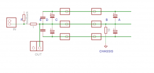
This is what I try to achieve. A-B PSU, the rest is the amp board.
I follow a similar layout, except i dispense with the 1ohm resistor as it induces a output error voltage (albeit small) when referenced to the input voltage. In order to minimize ground loop area, i prefer to join the supply earth and the chassis earth at the input signal ground.
This leads to a dead silent amplifier, no hiss or hum.
- Home
- Amplifiers
- Solid State
- Bob Cordell's Power amplifier book