Thank you.Mark you should have filtered the list to the ones that are applicable. Here is one from Gosser on the two stage CFA which as they say is obviously applicable to a VFA.
I am concerned, that in the point base Q5 with its high impedance is introduced the capacity of the Miller Ccb Q7, because this stage has high gain. It appears that the method of controlling the emitter currents of less distorts the frequency response of the amplifier.
Alas, Bob, the time of complex amplifiers have passed. To blame our education system, that produced more bolts for the system, and not independent researchers.There are indeed numerous ways to stabilize the VAS bias current in that arrangement, some more complicated than others. Mine is just one of the simpler ones.
Cheers,
Bob
I think the resistance load of the LTP is equal to 4.7 K. This is the right way to use the transistors 9, 10, 11 and 12, 13, 14 of the current mirror without benefits.More to the point Bob's final input stage is fine, the 4.7k resistors soak up the inevitable offset currents without causing large changes in the common mode bias current.
This is the right way to use the transistors 9, 10, 11 and 12, 13, 14 of the current mirror without benefits.
I don't agree, the DC gain reduction is no different than if the VAS had a DC source resistance of 4.7k but using the current mirror guarantees that the other end of the 4.7k see's the right voltage for balance at 0 input. The current mirrors still give the differential-in to two out of phase single ended outputs that you want. I suspect there is still more than enough open-loop gain.
I measured a bunch of PNP transistors and calculated that figure of merit; it's in column "L" of the table below.
Hi Mark, have you done a similar exercise for NPN transistors?
Hi!I don't agree, the DC gain reduction is no different than if the VAS had a DC source resistance of 4.7k but using the current mirror guarantees that the other end of the 4.7k see's the right voltage for balance at 0 input. The current mirrors still give the differential-in to two out of phase single ended outputs that you want. I suspect there is still more than enough open-loop gain.
This can be checked on the model.
An externally hosted image should be here but it was not working when we last tested it.
Here {R} is load the LTP. We change the resistor value from 20 to 1 K with step 1 K and LTS plots of gain.
I couldn't get the correct picture according to the method of Tian. Therefore, in the first approximation, assume that the open loop gain is inversely proportional to the voltage at the inverting input of the amplifier. This graphic we see.
An externally hosted image should be here but it was not working when we last tested it.
Attachments
Last edited:
the single Vsource loop gain test will work "perfectly" with your idealized E1 0 Z output
and seems accurate enough in most audio PA applications cutting the loop between the output and any feedback components where the reverse transfer captured by Tain or advanced Middlebrook dual injection techniques is typically negligible up to few MHz typical loop gain intercept frequencies
for sharing LTspice sims I sometimes just put any 3rd party Q models directly on the asc with the .op SPICE Directive
Last edited:
Hi!
This can be checked on the model.
What is being checked? Looks as I would expect above 5K or so there are diminishing returns (this is still not Bob's circuit). If you add offset trims to Bob's input stage (across the 180 Ohm resistors) you could probably increase the 4.7k to 50k (at least in sim) and quantify the difference in what was presented.
I got a ready-made model (I posted earlier). This model was to check the gain simplified installation mathematical multiplier of 1 (E1) instead of the output followers. I think, it is not critical for accuracy.the single Vsource loop gain test will work "perfectly" with your idealized E1 0 Z output
The stabilization of the current VAS could not be achieved by a simple installation of the resistor/s.
Yes it can and to do it we sacrifice open-loop gain, I'm not following your reasoning. Bob's circuit works plain and simple, some of the other techniques work best when you can area ratio devices on an IC and they work less well when you balance voltage drops across resistors with Vbe's. Bob's mirror and Vas balance two Vbe's against each other with a resitor drop in each path, this tends to be very stable over temperature. Your example runs ~1mA through a 680 Ohm resistor and one Vbe to match the two Vbe's in the Darlington Vas this is inherently not temperature stable. To repeat you have to simulate Bob's circuit not one you make up.
Last edited:
I thought I had lost this in a computer crash. I posted this here at least 5yr. ago. I built one and it works fine. If you trim the two mirrors on the input stage you have two degrees of freedom the offset can be trimmed to 0 while Aol trimmed to infinite or drift and offset trimmed to 0. I posted some scope plots of of the Aol going plus 1M through infinite to even -1M. The fully bootstrapped differential Vas (actually doubly differential) enables the trimming of Aol which has become simply the difference between large things and the user can trim the difference to zero +-.
Attachments
Last edited:
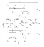
I have a few additions.
You need to set the stage with a common base in the drains of transistors LTP, area 1. This will reduce the voltage signal on the drains and thus reduce the parasitic connection between the drains and gates through capacitance drain-gate. It really works.
Also in the emitter circuit of the second LTP for linearity more favorable current source with high output impedance, area 2.
To reduce the nonlinearity of the input when receiving the signal from sources with a large output impedance (volume control) it is necessary to provide for the input transistors work floating voltage of the drain (collector), area 3.
Input stage requires to increase loop gain a high impedance of his load. Also need to reduce the parasitic Miller capacitance using Ccb Q72 (in my drawing - VT17). Followers on the input of the second cascade will cope with these two tasks, zone 4.
If you do this, gain input stage will increase to 20,000 times. It's a good idea to get opamp instead of transistors?
In your picture the resistors R5 and R6 harm, but not help.
I think, that you need to know: the signal at the emitters of Q1 and Q95 should be fed in-phase, and not paraphase.
I'll be glad if it helps you. Happy New Year!
You need to set the stage with a common base in the drains of transistors LTP, area 1. This will reduce the voltage signal on the drains and thus reduce the parasitic connection between the drains and gates through capacitance drain-gate. It really works.
An externally hosted image should be here but it was not working when we last tested it.
Also in the emitter circuit of the second LTP for linearity more favorable current source with high output impedance, area 2.
To reduce the nonlinearity of the input when receiving the signal from sources with a large output impedance (volume control) it is necessary to provide for the input transistors work floating voltage of the drain (collector), area 3.
Input stage requires to increase loop gain a high impedance of his load. Also need to reduce the parasitic Miller capacitance using Ccb Q72 (in my drawing - VT17). Followers on the input of the second cascade will cope with these two tasks, zone 4.
If you do this, gain input stage will increase to 20,000 times. It's a good idea to get opamp instead of transistors?
In your picture the resistors R5 and R6 harm, but not help.
I think, that you need to know: the signal at the emitters of Q1 and Q95 should be fed in-phase, and not paraphase.
I'll be glad if it helps you. Happy New Year!
Last edited:
I have a few additions.
You need to set the stage with a common base in the drains of transistors LTP, area 1. This will reduce the voltage signal on the drains and thus reduce the parasitic connection between the drains and gates through capacitance drain-gate. It really works.
An externally hosted image should be here but it was not working when we last tested it.
Also in the emitter circuit of the second LTP for linearity more favorable current source with high output impedance, area 2.
To reduce the nonlinearity of the input when receiving the signal from sources with a large output impedance (volume control) it is necessary to provide for the input transistors work floating voltage of the drain (collector), area 3.
Input stage requires to increase loop gain a high impedance of his load. Also need to reduce the parasitic Miller capacitance using Ccb Q72 (in my drawing - VT17). Followers on the input of the second cascade will cope with these two tasks, zone 4.
If you do this, gain input stage will increase to 20,000 times. It's a good idea to get opamp instead of transistors?
In your picture the resistors R5 and R6 harm, but not help.
I think, that you need to know: the signal at the emitters of Q1 and Q95 should be fed in-phase, and not paraphase.
I'll be glad if it helps you. Happy New Year!
VT16/17 (4)are called supper pair or Boxall or Baxandall, and not simple emitter follower.
Yes. I sought to minimize its input capacitance. This pair also showed the best results on the linearity. According to the model, THD this cascade for differential input - 0.6% for 20kHz. And it's not bad. It is only 6 dB worse, than THD in the cascade with a common base.
Last edited:
I think when you say 'model' you actually mean the whole circuit, right?
No, I was talking about distortion of one of the cascade. These distortions we can easily see through the natural work of NFB. Suppose, that the output of the amplifier THD = 0 or tends to zero, which is usually performed. Then THD on input from the last of the cascade will be equal THD this cascade. It is necessary for the fulfillment of the conditions output THD = 0. You and I understand, that this is a qualitative, estimated assessment. We make changes in circuit and the value THD shows, goog this or bad.
I showed earlier, how this works in the model for any cascade. To assess THD differential stage (LTP) can take E1.
Attachments
Last edited:
No, I was talking about distortion of one of the cascade. These distortions we can easily see through the natural work of NFB. Suppose, that the output of the amplifier THD = 0 or tends to zero, which is usually performed. Then THD on input from the last of the cascade will be equal THD this cascade. It is necessary for the fulfillment of the conditions output THD = 0. You and I understand, that this is a qualitative, estimated assessment. We make changes in circuit and the value THD shows, goog this or bad.
I showed earlier, how this works in the model for any cascade. To assess THD differential stage (LTP) can take E1.
This is what I referred to as input-referred distortion analysis.
It is especially useful in assessing the distortion of the output stage, in-situ, with the feedback loop closed. If the closed-loop output distortion is very low compared to the distortion of the output stage (as a result of the global NFB), then the distortion seen at the input to the output stage is that pre-distortion required to make the output distortion nearly zero. The distortion waveform at this point is merely an inverted approximation to the distortion of the output stage.
Cheers,
Bob
Yes. Because of the magnitude of the distortion, introduced by the cascades, are very different, we can see distortion of any of the cascades. For example, if we equate the distortion of the output follower to zero, the distortion of the VAS will be clearly visible.This is what I referred to as input-referred distortion analysis.
Happy New Year, Bob! Happy New Year to all!
Last edited:
- Home
- Amplifiers
- Solid State
- Bob Cordell's Power amplifier book