Kgrlee, yes I know all that but it's not easy to implement it to make perfect layout. I followed many discussion how to make good audio layout and this amp is my attempt to achieve all that, how good I am not sure.
Maybe you can comment on this layout, it is the one where I hope that distortion could go down when the boards are wired inside the chassis?
I look at your layout briefly as I don't have your schematic. I love laying out pcb, it's like a jigsaw puzzle for me. So excuse me of jumping in to this discussion.
1) I would do alternate P and N MOSFET so the current draw be P and N FET stay local ( 4 pairs local). With abundant of filter caps, the current pretty much travel through the ground trace between adjacent P and N pairs. The way you do it, huge current has to travel back and fore the length of the board.
2) I like that you have a large electrolytic in parallel with a small film or ceramic cap for power supply filtering. But I would switch the big and small cap. I would want to small cap that has lower series inductance to be as closed to the Drain pin as possible.
3) I would make the power and ground trace a lot wider.
I just did my OPS board as I described. I have 5 pairs of BJT power transistor. It is hard, but it can be done and I did it. Ground plane is at least 1" wide at all point along the long pcb, power planes that are at least 1/2" and output plane 3/4" wide. It can be done, just hard. This is not something you can tape and etch, I design on pcb layout package and sent the gerber to Hong Kong to fab. 10 pcs 2mm thick for $110. It's a 3Wks turn.
I also have the bias generating transistor mount directly on one of the power transistor also to get close track of temperature.
This is my layout in post #109: http://www.diyaudio.com/forums/solid-state/268265-please-comment-my-ops-design-11.html
Post#101 showed where I put the bias generating transistor Q9 on top of one of the power transistor Q17 to achieve faster thermal response time.
Last edited:
.Kgrlee, yes I know all that but it's not easy to implement it to make perfect layout. I followed many discussion how to make good audio layout and this amp is my attempt to achieve all that, how good I am not sure.
Maybe you can comment on this layout, it is the one where I hope that distortion could go down when the boards are wired inside the chassis?
Ok , I waited for Kgrlee's response.
You already are using double sided parallel tracks for your V+/V- (rails). You could improve
what you already have by alternating P/N/P/N output devices and continuing both
rails down the entire length of the board. PASS , Accuphase , hi-end luxmans
do this to provide rail emf cancellation across the whole PCB length.
The "silicon chip" blameless with thermaltraks also has this layout method.
Having that long decoupling return down the length of the board is counter-productive.
Better to have just two larger caps for decoupling at one end of the board
with very short fat tracks to a star (your GND faston). Having your servo ground
and other grounds on the right side of the board connecting to that "dirty" long
return also is not optimal.
A parallel double sided rail scheme with alternating outputs combined with a
grounding scheme like the forum's "badger" would assure your IPS would see
almost no iinducted "contamination". The output coil could go vertical , as well.
Look up a drawing of the field of a air core inductor - field comes out the end.
Or a PC CPU PS inductor , always perpendicular to the ground plane or any other
traces.
Not an expert by any means on these techniques. I learned by studying the
layouts of the >5K$ hi-end units (reverse engineering). This is how they
get that level of performance.
OS
Last edited:
I don't buy into people judge the amp by the price and the looks.
Well, those people who made the effort to look into that fond that it IS the case, often to their dismay. Like the differences between speaker ratings between seeing what speaker is playing or not seeing it. Even the designers who boasted that they knew how to circumvent their own prejudices couldn't!
See, for instance, page 10, 'BLIND vs. SIGHTED TESTS – SEEING IS BELIEVING' in http://linearaudio.nl/sites/linearaudio.net/files/floyd o'toole AudioScience.pdf .
Or 'The dishonesty of sighted listening tests' in Audio Musings by Sean Olive: The Dishonesty of Sighted Listening Tests .
Jan
But what make you think the spectrum analyzer can tell whether the amp sounds good?
No idea. Can it? I doubt that. A spectrum analyzer can tell you the relative spectrum of frequencies in a signal. I don't see a correspondence from that to sound quality.
Jan
I am not saying all the test equipment are useless, it's just the final judge is still the ears. Seems like a lot of people only talk in terms of spectrum and slew rate, I think that misses the point.
I think that sound of the YBA is jaw dropping, but if you look at the schematic, it's very simple, it's nothing. I bet people will laugh if they look at the spectrum. It looked cheap also.
There is some truth about less is more, this is particular true for guitar amp. You can have all the stages to shape the sound, but along the way, the sweetness of the guitar sound got lost. The best sounding amp are still the really simple ones with minimal gain stages. Krell and Mach and known to be anal in lowering distortion, circuit are always complicated. I am not impressed with sound of neither one. They sound dead to me, just like the guitar amp with many gain stages that sound dead to me.
Last edited:
I am not saying all the test equipment are useless, it's just the final judge is still the ears.
Of course, that goes without saying, as long as you mean 'the final judge of sound quality is the ears'. Test equipment is very useful when developing an amp towards the goals you have set yourself in technical terms.
But the fact is that people prefer one amp over the other based on a whole slew of factors, of which objective sound quality is just one. I think the examples I linked to above make that very clear.
And let's face it, in our gut we know that many factors determine whether we like one thing over another. Change the context and we may well like a different thing more or less.
There's a multi-trillion euro industry based on that, it's called 'marketing'
")
Jan
Last edited:
Dadod, I have to admit this PCB is very close to how I would do it.
In particular, all the high current flows in what is almost a bunch of twisted wires.
Thank you kgrlee. I can see that you have a new occupation: Pandit Litoral @ Cooktown Recording and Ambisonic Productions?
I look at your layout briefly as I don't have your schematic. I love laying out pcb, it's like a jigsaw puzzle for me. So excuse me of jumping in to this discussion.
1) I would do alternate P and N MOSFET so the current draw be P and N FET stay local ( 4 pairs local). With abundant of filter caps, the current pretty much travel through the ground trace between adjacent P and N pairs. The way you do it, huge current has to travel back and fore the length of the board.
2) I like that you have a large electrolytic in parallel with a small film or ceramic cap for power supply filtering. But I would switch the big and small cap. I would want to small cap that has lower series inductance to be as closed to the Drain pin as possible.
3) I would make the power and ground trace a lot wider.
I just did my OPS board as I described. I have 5 pairs of BJT power transistor. It is hard, but it can be done and I did it. Ground plane is at least 1" wide at all point along the long pcb, power planes that are at least 1/2" and output plane 3/4" wide. It can be done, just hard. This is not something you can tape and etch, I design on pcb layout package and sent the gerber to Hong Kong to fab. 10 pcs 2mm thick for $110. It's a 3Wks turn.
I also have the bias generating transistor mount directly on one of the power transistor also to get close track of temperature.
This is my layout in post #109: http://www.diyaudio.com/forums/solid-state/268265-please-comment-my-ops-design-11.html
Post#101 showed where I put the bias generating transistor Q9 on top of one of the power transistor Q17 to achieve faster thermal response time.
Than you Alan to spare some time for this layout.
1) I started some time ago to layout the OPS in this way. It is more complicate and needs more board space and I didn't finish it yet.
How much that will improve the amp I am not sure.
2) Actually I made provision for parallel small cap with the big one but did not solder them, so the boards delivered to Richard are without them. This is a bit controversial as some say it could make more damage then improvement. In my Thermal Trak VFA amp I did solder small ceramic caps parallel to the big ones directly from the bottom side and could not sax if it's better with them or without them. Maybe Richard can tray some small caps there, he is much better caps expert than I ever be.
3) I used 2 OZ copper and this is not PA to play very loud all the time, but an amp for domestic listening and some short loud transient will not damage the power tracks. To make those traces much wider will change the layout to much to my liking, always is possible to add some copper bars to those tracks. I, always try to make the feedback track as short as possible.
I don't think that is important to mount the Vbe multiplier directly on one output VMOSFET as mosfets are not to much sensitive to the bias current change. For the BJT OPS is more important, that's way I prefer Thermal Trak there.
BR Damir
.
Ok , I waited for Kgrlee's response.
You already are using double sided parallel tracks for your V+/V- (rails). You could improve
what you already have by alternating P/N/P/N output devices and continuing both
rails down the entire length of the board. PASS , Accuphase , hi-end luxmans
do this to provide rail emf cancellation across the whole PCB length.
The "silicon chip" blameless with thermaltraks also has this layout method.
Having that long decoupling return down the length of the board is counter-productive.
Better to have just two larger caps for decoupling at one end of the board
with very short fat tracks to a star (your GND faston). Having your servo ground
and other grounds on the right side of the board connecting to that "dirty" long
return also is not optimal.
A parallel double sided rail scheme with alternating outputs combined with a
grounding scheme like the forum's "badger" would assure your IPS would see
almost no iinducted "contamination". The output coil could go vertical , as well.
Look up a drawing of the field of a air core inductor - field comes out the end.
Or a PC CPU PS inductor , always perpendicular to the ground plane or any other
traces.
Not an expert by any means on these techniques. I learned by studying the
layouts of the >5K$ hi-end units (reverse engineering). This is how they
get that level of performance.
OS
Os, I always appreciate your opinion, many thanks.
From the answer to Alan you N and P devices on my next improved layout.
Regarding two big caps instead distributed smaller ones I disagree.
Output coils on that layout is optional as I provided direct output faston connector in case someone wants to have that coil remotely installed.
And there is quite large alu heat sink for the drivers between the coil and the input circuitry and I think it protect it as the coil is perpendicular to it.
There two grounds there, dirty ground where all big power caps are connected and the signal ground where input, feedback and compensation is connected, even servo input cap is connected there. I was in dilemma where to connect small servo elcos and decided better to connect to the dirty ground.
Your concept how to organize the layouts is different than mine. You like to have separate boards for IPS and OPS. I think that short feedback connection is paramount for good amp and that requires one board for whole amp (exception is small board with the feedback resistors as for CFA there is need for power there). I also think to get the best from one configuration the IPS and the OPS should be designed for best play together.
BR Damir
3) I used 2 OZ copper and this is not PA to play very loud all the time, but an amp for domestic listening and some short loud transient will not damage the power tracks. To make those traces much wider will change the layout to much to my liking, always is possible to add some copper bars to those tracks. I, always try to make the feedback track as short as possible.
It is not about whether the trace can handle the current, it's about narrow trace have much higher inductance and it can become parasitic inductance. The output stage is very low impedance, you don't need much inductance to become significant at high frequency.
Also, if you look at the layout, you have space between the power and ground and also the output trace, this will form a magnetic loop and magnetic field will come out. magnetic field proportion to the current through the trace and the loop area between. So it's not a good thing.
I don't think that is important to mount the Vbe multiplier directly on one output VMOSFET as mosfets are not to much sensitive to the bias current change. For the BJT OPS is more important, that's way I prefer Thermal Trak there.
BR Damir
Yes, my bad, I forgot this is MOSFET that does not need temperature tracking. I use BJT, it's critical for me.
Can you post the schematic of the YBA please?I think that sound of the YBA is jaw dropping, but if you look at the schematic, it's very simple, it's nothing.
My Holy Grail is to achieve 1pp zillion THD with very simple circuits. My prejudice is that this will give good sound cos it is amenable to rigorous analysis, testing and there is less to go wrong.
Just to add to Olive & Co. ...But the fact is that people prefer one amp over the other based on a whole slew of factors, of which objective sound quality is just one. I think the examples I linked to above make that very clear.
Objective sound quality MUST be judged with DBLTs. If you do this carefully, you'll find that most (all?) self declared Golden Pinnae, including most HiFi Reviewers are deaf. They give random results in DBLTs.
If you do them long enough, you may be lucky to find some true golden pinnae. They are likely to be people you least expect like your girlfriend, wife or mother.
But even the best golden pinnae are just as prejudiced and opinionated as the most raving audiophool. There are people whose opinion I trust in DBLTs ... but discount heavily in sighted tests. One of them is the rare golden pinnae who is also a HiFi reviewer and in fact the editor of a major magazine.
___________________
In ALL cases where I've found a reliable preference of my DBLT panel on amps, one or other of the amps was marginally unstable with real life loads with bursts of oscillation on part of the waveform .. all depending on the thermal and signal history.
Then, I would claim that ALL Golden Pinnae amps including some designed by famous names in this forum were only marginally stable. This Millenium, my opinion of these famous name designs is only confirmed but I don't test as many amps as I used to.
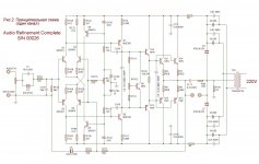
On Damir's PCB from #5225 ...
- there's an advantage in alternating P & N channel output devices but its likely small.
- I can't see how he could get the high current earth return any closer to his high current rails
- But the biggest advantage compared to the Badger layout is that it has the VAS & i/p as close as possible to the outputs. Toni's (astx) 200W amp is a very refined version of Badger and in trying to sim some of his 'real life' results, it is obvious that the connection between the 'driver' PCB and the output PCB is a major reason for the sims not reflecting 'real life'
- The only change I might ask for is that the dirty earth to the clean earth not be taken right round the PCB. Its an alternative path for the high currents and is also a 'loop'. It's not clear if this loop is complete.
Hello kgrlee,
Nice to see your post. I wonder if some singers who have perfect pitch would be good at dblt, not sure if it would carry over that way. Most musician I have known don't even seem to care about the sound, they just listen differently to the music, they seem more into the composition than the actual sound.
Nice to see your post. I wonder if some singers who have perfect pitch would be good at dblt, not sure if it would carry over that way. Most musician I have known don't even seem to care about the sound, they just listen differently to the music, they seem more into the composition than the actual sound.
You will be very disappointed, the distortion is going to be high. Only 33ohm degeneration resistor, no cascode on LTP, no darlington VAS and 2EF. That's the hallmark of a cheap amp.Can you post the schematic of the YBA please?
My Holy Grail is to achieve 1pp zillion THD with very simple circuits. My prejudice is that this will give good sound cos it is amenable to rigorous analysis, testing and there is less to go wrong.
To me, distortion means nothing. It's the sound. I don't care to even debate tube or SS. It's the sound and that's the only thing that matter.
- there's an advantage in alternating P & N channel output devices but its likely small.
- I can't see how he could get the high current earth return any closer to his high current rails
Current is push pull between P and N. You have P on one side and N on the other side. Current travel the whole length of the board. With P N alternate, the current loop is only on each pair. This is local current loop. This is particular important if you have thin trace.
I worked with MOSFET for years, not on audiophile. If it is done correctly, they are very rugged. But if you are not careful and leaving parasitic at the drain and gate path, they tend to oscillate and burn the gate very fast. They die a very quiet death. You turn on, it just die.....cold. You measure, everything shorted. Seen this too often already. Layout is very important and you have to treat it as RF device.......as they are. They are being used in RF power amp by making use of their Cgs capacitance for tuning. That's the reason I decided against using MOSFET myself even with all the supposedly advantage and stay with BJT. The last one I burn was used in my power scaling design for a tube guitar amp last year. You leave the lead a little long, you might get into trouble. By long, I mean 1", not a few inches.
You cannot use zener, transorbs to clamp the gate, it's internal. we tried it all. Only cure is short thick wires. You treat it as RF device, they last and last.
Attachments
Last edited:
On Damir's PCB from #5225 ...
- there's an advantage in alternating P & N channel output devices but its likely small.
- I can't see how he could get the high current earth return any closer to his high current rails
- But the biggest advantage compared to the Badger layout is that it has the VAS & i/p as close as possible to the outputs. Toni's (astx) 200W amp is a very refined version of Badger and in trying to sim some of his 'real life' results, it is obvious that the connection between the 'driver' PCB and the output PCB is a major reason for the sims not reflecting 'real life'
- The only change I might ask for is that the dirty earth to the clean earth not be taken right round the PCB. Its an alternative path for the high currents and is also a 'loop'. It's not clear if this loop is complete.
I suppose you mean #5255.
The dirty earth does not go in a loop, it is just takes the ground connections of the input stage elcos and there the current is small and not very variable. The clean earth is below in the middle connected internally via 10R resistor to the dirty earth, but should be connected via faston connector (signal ground) to the main star ground point where all other ground wires are connected, between them the return loudspeaker wire too.
To me, distortion means nothing. It's the sound. I don't care to even debate tube or SS. It's the sound and that's the only thing that matter.
This is very contradicted statement. Distortion is just that what it says, distortion, change of original sound. It was discussed many times and I don't want to start that again. High distortion amplifiers can sound nice with some kind of simple music, but hardly with big orchestra and classic music, and that is not High Fidelity.
On Damir's PCB from #5225 ...
- 1. there's an advantage in alternating P & N channel output devices but its likely small.
- 2.I can't see how he could get the high current earth return any closer to his high current rails
- 3.But the biggest advantage compared to the Badger layout is that it has the VAS & i/p as close as possible to the outputs. Toni's (astx) 200W amp is a very refined version of Badger and in trying to sim some of his 'real life' results, it is obvious that the connection between the 'driver' PCB and the output PCB is a major reason for the sims not reflecting 'real life'
1. But then he could have both rails running down the whole length of the board -
cancellation. If he kept the caps at each output it would also be a shorter current
loop between +/- .
2. It could be done.
3. ASTX's amp was studied (by me). You speak of those long leads. He does
run an EF2 and lower Z VAS than my slewmaster EF3 , but foot-long connections
are quite excessive. I don't recommend anything over 50mm , my input stage
output is 35-40mm from the first EF3 predrivers. Cap multiplier outputs just
25mm from the input stages first decoupling caps - real close.
Saw a Halcro layout , also has the input stage regulators and input stage with a
separate ground return from the "dirty" output stage one.
Then there is the "YAP" amp - The YAP Output Stage
This was my "ground zero" inspiration for the badger and especially the
slewmaster. Separate OPS/IPS - then the "PGP" amp with EC @ 1/2ppm 20K
uses rail stars and a central ground star - Schematics
Real good stuff - and really measures good , too !
PS - some of these boys quit the forum , cause we be a bunch of "dummies"
OS
- Home
- Amplifiers
- Solid State
- Bob Cordell's Power amplifier book