Could use a smaller RE, 0,1 Ohm would +- 25mA.
Forgot to mention in the previous topic, CFP output decreases NFB in 40% with load, surely this is problem, had an amp released here in the 70s that had this problem, DF decreases with load, when the volume increases, the bass were "floppy".
VBE multiplier is a big problem, even if you use ThermalTrak (are more costly) still have the problem of having "two bias" one for winter where the amplifier operates more cold and other for the summer, dynamic bias control is necessary.
I like the BJTs by having good symmetry PNP/NPN, but I believe that a Mosfet output would be the better choice, I will use in my next amp.
Hi Rafael,
An amplifier, especially a ThermalTrak, with a properly designed Vbe multiplier for bias control should not operate differently depending on the ambient temperature of its environment.
Cheers,
Bob
Hi AudioLapDance,
Sounds like you are referring the the basic amplifier that is evolved in Chapter 3 (the Evolution Amplifier?). Is that right?
The answer is that there is not. I have not had the time thusfar to do something like that. Darned day job.
But hmmmm... That is an interesting idea. Tempting...
Cheers,
Bob
No, the freak, way!?!

No one's suggested this? This would be a intro to DIY and amp design DREAM!!11! I could even write-up a high-school course or summer camp around this!
Ya, start with the basic circuit, get used to it and then: next problem-next improvement, listen; next problem-next improvement, listen ... To walk through step-by-step, with the solid circuit analysis, technical descriptions and overall engineering methodology, would be extraordinarily educational!
If we could add in what to listen for (specific songs), the linking of 'this distortion sounds like that' and 'this circuit shortcoming produces this effect on big dynamics' would be ... again, enlightening.
Oh, and note I said 'Cordell approved.'
I did not mean to suggest that you personally design a PCB but perhaps a current contributor (competent layout artist) can give it a go and get your oversight and final stamp. I greatly appreciate your DIY contributions and would not want to overly tax your time.
(Even the layout back-and-forth would be neat)
Pleased to meet you Sir!
Cheers,
Jeff
PS And same with your more complex chipamp! Buffer sounds like this, inverted sounds like that, advanced zobels sound like that ... awesome!
Last edited:
Bob, suppose you have designed your amp to operate at a temperature of 40°C and drivers in 45°C, but in summer, temperature internal rises 5° C, for all transistors 45° C and 50°C for drivers.Hi Rafael,
An amplifier, especially a ThermalTrak, with a properly designed Vbe multiplier for bias control should not operate differently depending on the ambient temperature of its environment.
Cheers,
Bob
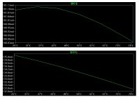
Simulating these temperatures in my circuit:
LTP 2,95mA-40°C, 3mA-45°C
VAS 4,44mA-40°C, 4,61mA-45°C
If not adjust the trimpot would take over bias, see the graph:
Attachments
Jeff,
I think that a few of us would love to see the same thing. An amplifier optimized for easily acquired device so the end result will be a stable design. I know that on other threads a third party here has done all the board layout following direction and discussion. The board would be an addendum to Bob's book, what a way to get it right.
I think that a few of us would love to see the same thing. An amplifier optimized for easily acquired device so the end result will be a stable design. I know that on other threads a third party here has done all the board layout following direction and discussion. The board would be an addendum to Bob's book, what a way to get it right.
I like that configuration, I just try to do as good with less parts.
One option is to increase Vce, the other is to decrease the knee, by choosing a better device.
One possibility with less parts is to use a Current Mirror helper transistor and just put a resistor in the emitter. Perfectly obvious after I had the idea, but I've never seen it. Anyone else done this?
Best wishes
David
Jeff,
I think that a few of us would love to see the same thing. An amplifier optimized for easily acquired device so the end result will be a stable design. I know that on other threads a third party here has done all the board layout following direction and discussion. The board would be an addendum to Bob's book, what a way to get it right.
I thought of the addendum ... and was actually fantasizing about a BCEvo Amp PCB, BCchipamp PCB and step-by-step test track CD included with the next issue of the book ... but that's a bit presumptuous on my part
Let's just get a quick, simple, easy PCB going!
Would a new thread be in order?
Last edited:
One possibility with less parts is to use a Current Mirror helper transistor and just put a resistor in the emitter. Perfectly obvious after I had the idea, but I've never seen it. Anyone else done this?
Best wishes
David
You mean the buffered CM? Normally Zcb is doubled by current mirror action. If the buffer has less Rm than the mirror pair, Zcb will be less then doubled, so there can be no more than a 6db advantage to this configuration AFAIK. The cost of that gain will be the Iq needed to maintain low buffer Rm, which will be >> than one of the CM transistors. Furthermore, I've heard complaints about this kind of mirror having peaky gain and possible stability issues. [this is all moot if Zcb is not the dominant error source...]
If the above is heeded, the buffered CM would put Vce of the output transistor no lower than an ordinary CM. If your goal were Vce matching, it would allow you to give the output transistor an extra diode drop to match the sense transistor. So you would end up with a matched CM further away from saturation. At the same time, degeneration would need to decrease, and this may lose us what we gained. [I am not sure how much Vce improves Vbe modulation for a CM; it didn't seem very significant in my Kmultiplier experiments, or in simulations, so reducing degeneration in this case only make things worse while increasing Vce helps nothing]
What about a Wilson mirror, with an extra diode to balance Vce's? Since both Vce's will be constant, Vbe modulation is not an issue. Vce of all transistors will be reduced, but so will the corresponding distortions, except for Zcb of the third transistor.
In the simulator this appears to apply. Because quasi-saturation is so low the BC5x0 and BC3x7 models behave close to real life based on my Kmultiplier experience, so I trust these simulations. I found an error improvement of 17db over the ordinary 2-transistor mirror with 1420mV degeneration, using a wilson mirror with 47R degeneration. This shows Vbe modulation is effectively eliminated. The buffered mirror is not an improvement over the non-buffered mirror. So even with 1420mV degeneration, Vbe modulation is the dominant error source, not Zcb. I define error as (Iin-Iout)/Iin. In the design being simulated, the improved mirror resulted in not more than an improvement of 5% of the total THD.
These results are specific to astx's amplifier, so are not broadly applicable.
I knew there was a reason I never preferred the buffered CM.
Last edited:
I fail to appreciate how increasing TIS Gm can improve stability of the minor loop.
I didn't say that it improves the stability of the minor loop but the stability of the major loop.
IMHO, the minor loop loop gain phase margin is not affected by change in gm vas for a miller compensation, it can be shown that it remains 90°. Of course any reactive load influences that loop gain.
The closed loop poles of the minor loop are the poles of the loop gain of the main loop. These poles are subject to pole splitting with C miller and gm vas, widening them improves overall stability.
Stability problems of the minor loop due to reactive loading is tricky because compensation is then related to a specific load. You can end up in a compensated amplifier with good margin but requiring a capacitive load. If the capacitive load is removed, the amplifier looses its margin. see Lundberg paper for a very nice analysis
You mean the buffered CM? Normally Zcb is doubled by current mirror action. If the buffer has less Rm than the mirror pair, Zcb will be less then doubled, so there can be no more than a 6db advantage to this configuration AFAIK. The cost of that gain will be the Iq needed to maintain low buffer Rm, which will be >> than one of the CM transistors. Furthermore, I've heard complaints about this kind of mirror having peaky gain and possible stability issues. [this is all moot if Zcb is not the dominant error source...]
If the above is heeded, the buffered CM would put Vce of the output transistor no lower than an ordinary CM. If your goal were Vce matching, it would allow you to give the output transistor an extra diode drop to match the sense transistor. So you would end up with a matched CM further away from saturation. At the same time, degeneration would need to decrease, and this may lose us what we gained. [I am not sure how much Vce improves Vbe modulation for a CM; it didn't seem very significant in my Kmultiplier experiments, or in simulations, so reducing degeneration in this case only make things worse while increasing Vce helps nothing]
What about a Wilson mirror, with an extra diode to balance Vce's? Since both Vce's will be constant, Vbe modulation is not an issue. Vce of all transistors will be reduced, but so will the corresponding distortions, except for Zcb of the third transistor.
In the simulator this appears to apply. Because quasi-saturation is so low the BC5x0 and BC3x7 models behave close to real life based on my Kmultiplier experience, so I trust these simulations. I found an error improvement of 17db over the ordinary 2-transistor mirror with 1420mV degeneration, using a wilson mirror with 47R degeneration. This shows Vbe modulation is effectively eliminated. The buffered mirror is not an improvement over the non-buffered mirror. So even with 1420mV degeneration, Vbe modulation is the dominant error source, not Zcb. I define error as (Iin-Iout)/Iin. In the design being simulated, the improved mirror resulted in not more than an improvement of 5% of the total THD.
These results are specific to astx's amplifier, so are not broadly applicable.
I knew there was a reason I never preferred the buffered CM.
I suppose that what you call bufferd CM is what Cordell calls improved CM. My simulation does not support your claim about Wilson CM aganst improved CM. I simulated both in my GainWire preamp(current conveyor).
Improved CM at 11Vpp output (before output buffer) THD20k=0.000227%
Wilson CM at 11Vpp -''- THD20k=0.000308%
Can you post a link to the schematic?
In your circuit the current mirrors must be linear over a wide current range. The same is not true of a CM in astx's amp. Here the main distortion mechanism is CM output impedance.
Also, what about the 1K distortion figures? Output capacitance of a current mirror is doubled by CM action, unless you use a buffered CM where the buffer's Rm is << than that of one side of the CM.
Can you post a link to the schematic?
In your circuit the current mirrors must be linear over a wide current range. The same is not true of a CM in astx's amp. Here the main distortion mechanism is CM output impedance.
Also, what about the 1K distortion figures? Output capacitance of a current mirror is doubled by CM action, unless you use a buffered CM where the buffer's Rm is << than that of one side of the CM.
Here first improved CM, second Wilson CM
Damir
Attachments
Well it's already cascoded with a Baxandall, so there's not much you can do to improve it. The Widlar and Wilson mirrors only apply when the output is not cascoded IIRC. If you need very strict matching you may want to use a Wilson. But it's hard to predict what all of this will do to linearity, especially in real life for a circuit which utterly depends on the current mirror linearity. What is THD with just a normal mirror?
With the wilson, add a diode in series with the Q1 collector to see if that brings it back to normal. The Vce's are unbalanced with the Wilson; what I proposed included a diode to fix that. Also notice that the way the cascode is connected, the mirror is already very similar to a Wilson mirror.
With the wilson, add a diode in series with the Q1 collector to see if that brings it back to normal. The Vce's are unbalanced with the Wilson; what I proposed included a diode to fix that. Also notice that the way the cascode is connected, the mirror is already very similar to a Wilson mirror.
Last edited:
Well it's already cascoded with a Baxandall, so there's not much you can do to improve it. The Widlar and Wilson mirrors only apply when the output is not cascoded IIRC. If you need very strict matching you may want to use a Wilson. But it's hard to predict what all of this will do to linearity, especially in real life for a circuit which utterly depends on the current mirror linearity. What is THD with just a normal mirror?
With the wilson, add a diode in series with the Q1 collector to see if that brings it back to normal. The Vce's are unbalanced with the Wilson; what I proposed included a diode to fix that. Also notice that the way the cascode is connected, the mirror is already very similar to a Wilson mirror.
Normal mirror, same condition as before, THD20k= 0.000379%
Wilson mirror plus diode in series with the Q1, THD=0.000309% (same as without diode)
No, the freak, way!?!
No one's suggested this? This would be a intro to DIY and amp design DREAM!!11! I could even write-up a high-school course or summer camp around this!
Ya, start with the basic circuit, get used to it and then: next problem-next improvement, listen; next problem-next improvement, listen ... To walk through step-by-step, with the solid circuit analysis, technical descriptions and overall engineering methodology, would be extraordinarily educational!
If we could add in what to listen for (specific songs), the linking of 'this distortion sounds like that' and 'this circuit shortcoming produces this effect on big dynamics' would be ... again, enlightening.
Oh, and note I said 'Cordell approved.'
I did not mean to suggest that you personally design a PCB but perhaps a current contributor (competent layout artist) can give it a go and get your oversight and final stamp. I greatly appreciate your DIY contributions and would not want to overly tax your time.
(Even the layout back-and-forth would be neat)
Pleased to meet you Sir!
Cheers,
Jeff
PS And same with your more complex chipamp! Buffer sounds like this, inverted sounds like that, advanced zobels sound like that ... awesome!
Hi Jeff,
Thanks for your enthusiasm!
I'm guessing that such a board would be designed for the most complex version of the evolution, and would have component options to dumb it down to the simpler versions, perhaps requiring some jumpers in place of components, or components not installed for the lesser versions in the progression. This would probably not be difficult to do. However, if one is going to progress through the various incarnations, a moderate amount of component removal/replacement would be required along the way.
Does this fit with what you had in mind?
Cheers,
Bob
The comparison with the buffered CM is unfair because the output of the widlar is cascoded, whereas in astx's and in most other circuits it isn't. Remove the cascodes and then compare THD between the Wilson and buffered CM. I'm pretty sure the Wilson will outperform.
Same condition as before.
Ordinary CM THD20k=0.019543%
Improved CM THD20k=0.010530%
Wilson CM THD20k=0.021373%
Damir
is this an example of the Vsat models not being good, or that the vsat models are correct but that the device is not good as a mirror, or some other sim quirk?Same condition as before.
Ordinary CM THD20k=0.019543%
Improved CM THD20k=0.010530%
Wilson CM THD20k=0.021373%
Damir
Bob, suppose you have designed your amp to operate at a temperature of 40°C and drivers in 45°C, but in summer, temperature internal rises 5° C, for all transistors 45° C and 50°C for drivers.
Simulating these temperatures in my circuit:
LTP 2,95mA-40°C, 3mA-45°C
VAS 4,44mA-40°C, 4,61mA-45°C
If not adjust the trimpot would take over bias, see the graph:
Hi Rafael,
It looks like you may be missing the compensating effect of the Vbe multiplier transistor being mounted on the heat sink. If the room is hotter by 10C, then everything, including transistors and heatsinks, will be hotter by 10C, in principle. Then, if the thermal design and bias spreader are correctly implemented, bias should remain unchanged.
A good test for this is to put the entire amplifier in the oven and rig a couple of wires out so that you can monitor the quiescent output stage bias. Perhaps look at the voltage across RE of the output stage. Use 100-ohm probe isolating resistors at the attachment points to the output stage RE resistors so that if something goes wrong you wont smoke the amplifier.
Cheers,
Bob
No, I'm not forgetting the transistor compensation the VBE multiplier, I do not know if you know this feature in spice, locking all transistors/diodes in a fixed temperature. I lock all transistors for the temperature internal of case, only the output transistors and transistor sensor VBE are unlocked.
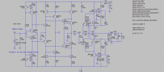
I forgot to mention in the previous topic, in my circuit use a triple output (T), pre drives and drives will not in heatsink.
Doing some simulations, found that the culprits by changing the bias current is the change of VBE pre-drives and drives, an increase of only 5°C you will have an increase of 30% in bias current of output transistors.
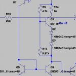
The circuit in Figure is my VBE multiplier for a triple (T), as I am not using ThermalTrak the circuit set for over-compensating in 10°C (40%), this difference in temperature between the transistor output and monitor VBE mounted on heatsink, this according to book D.Self (3 edition).
Attachments
No, I'm not forgetting the transistor compensation the VBE multiplier, I do not know if you know this feature in spice, locking all transistors/diodes in a fixed temperature. I lock all transistors for the temperature internal of case, only the output transistors and transistor sensor VBE are unlocked.
I forgot to mention in the previous topic, in my circuit use a triple output (T), pre drives and drives will not in heatsink.
Doing some simulations, found that the culprits by changing the bias current is the change of VBE pre-drives and drives, an increase of only 5°C you will have an increase of 30% in bias current of output transistors.
The circuit in Figure is my VBE multiplier for a triple (T), as I am not using ThermalTrak the circuit set for over-compensating in 10°C (40%), this difference in temperature between the transistor output and monitor VBE mounted on heatsink, this according to book D.Self (3 edition).
Hi Rafael,
I was not aware of this temperature locking feature in SPICE. Thanks for bringing it to my attention.
As we all know, 3EF Triples tend to be more difficult to temperature stabilize because there are a total of 6 junction drops effectively in series. One of my favorite approaches is to use two transistors in the bias spreader. One on the heatsink and one on a board-mounted heat spreader bar onto which are also mounted the pre-drivers and drivers.
Cheers,
Bob
- Home
- Amplifiers
- Solid State
- Bob Cordell's Power amplifier book