Oops, in the previous post I got the orange and red traces confused.
And here is the FFT and OLG plots for with TPC set at 2.5% overshoot. There is practically no difference in THD; shunt compensation has 3db less (I improved the compensation slightly since the last post). So much for local feedback. And this is with a buffered CE TIS.
And here is the FFT and OLG plots for with TPC set at 2.5% overshoot. There is practically no difference in THD; shunt compensation has 3db less (I improved the compensation slightly since the last post). So much for local feedback. And this is with a buffered CE TIS.
Attachments


My compensation scheme is like the schematic on page 85 of Cordell's book, except R7 is in series with C1 instead of C2.
Glad to see this thread alive again with some technical discussion, thanks.
As is often the case for me, I'm not 100% sure I am visualizing the intended circuit or implementation, specifically the above mentioned RC shunt compensation.
Since this is Bob's thread would it be possible to reference a specific figure(s) in his book? I would think that Bob would encourage and benefit from such a discussion.
Keantoken, your electronics insight is amazing for someone any age, but at your age its truly a gift.
Thanks
-Antonio
Hi Antonio,
I'm also glad to see this great discussion going on. I've been a bit out of the loop with a vacation and now a bad cold. The fuzzy head due to the cold medication makes it hard to make sensible comments.
Your observation about Keantoken is right on target.
Cheers,
Bob
Hi Guys
pg.85 has fig.4-5 showing lag compensation.
A series RC hangs from the VAS collector to ground. The zero in this network is supposed to cancel the pole for the input to the VAS. A second lag network is simply a cap to ground from the VAS base, which is also the output of the diff-amp.
Slew rate is low and asymmetrical with this approach, as Bob states. Basic miller compensation works better in his examples anyway.
Have fun
Kevin O'Connor
The RC is across the TIS input, and at the TIS output is a cap to ground, which is reversed from Bob's example. This configuration gives lower distortion and can have higher slew rate.
I noticed in Bob's example the TIS input cap to ground is totally wrong, this will inject supply noise right into the output, and the current loop for this cap has to go through all the decoupling caps to get back to the TIS emitter. The cap needs to be across the TIS input. Otherwise no wonder it doesn't work very well.
PS. This is a nice discussion Bob but I think I may have killed it!!!
Hi Guys
In the sequence of comp scheme drawings in Bob's book, the lag method of this figure (4-5) is the first, and presumably the worst yet simplest to understand. He describes it as "simplest" and "often not the best".
I think that because he seems so invested in the compensation scheme used in his mosfet amp (because it works so well!), there can be some "short hands" taken with other schemes that are not preferred. Hanging a cap to ground from the signal path is something one can think of loosely, and then the AC ground that is the reference for the VAS emitter becomes one and the same as real ground. However, in the real world these are quite different, as Keantoken pointed out. I think Bob just made a "colloquial equivalence" oversight there (proving that Bob is human).
Keantoken, when you described "across the TIS input" I envisioned it as you meant it as that is in line with my own preferred compensation schemes. It should also be intuitive for anyone to visualise who can picture schematics easily.
Have fun
Kevin O'Connor
The schematic on page 242 has something close enough to what I'm talking about, although there isn't a section on this alternate form of shunt compensation.
Hi Guys
Fig 11-17 (pg242) combines transitional comp with the favoured RC across the diff output, and lag RC from the VAS output to ground. The opne-loop circuits combine various compensation methods, as in fig.25-15. Lots of ways to achieve stability.
Have fun
Kevin O'Connor
Fig 11-17 (pg242) combines transitional comp with the favoured RC across the diff output, and lag RC from the VAS output to ground. The opne-loop circuits combine various compensation methods, as in fig.25-15. Lots of ways to achieve stability.
Have fun
Kevin O'Connor
"The Devil is in the details" is an often used English idiom meaning that small things in plans and schemes that are often overlooked can cause serious problems later on.
Some audio amplifier designers believe that "The Devil is is in the ground" and favor using compensation schemes which minimize ground connections. There are white papers for fully balanced audio amplifiers claiming that only power supplies and cable shielding should be connected to ground. A ground noise source is sometimes added to Spice simulations in these papers.
Example complementary differential amp design uses current mirrors, Hawksford VAS with TMC compensation, and triple-T output. LTSpice THD for 300W @8ohms is under 1ppm.
The first attached FFT uses a R+C across each input LTP to control high frequency oscillation. Note that the 2nd harmonic distortion is lower than the 3rd harmonic.
This complementary differential amplifier simulates with lower THD when, instead of the LTP compensation, an R+C is connected to each VAS collector and ground to control high frequency oscillation. On the second attached FFT, note that the second harmonic is larger than the third harmonic. No noise source is added to ground.
I have not found a complementary differential power amp schematic with a VAS solution for Kevin O'Connor's 4T Wilson CM. "I think one of the simplest solutions is to use the Wilson CM with fourth BJT added, as this sets both diff collectors at the same potential - or at least the collector in question has a set voltage."
Attachments


I thought that comment was sort of odd too. I know that often transistors with bad quasi-sat parameters are used in current mirrors, and this can lead to an effective CM shunt of as small as 500R. 47k resistor now possibly made terribly redundant. This would explain why a 4T Wilson mirror might work better - it gets both transistors equally into quasi-saturation - and perhaps the output side of the CM still has low enough Vce to have resistive shunt.
Of course in simulation you would never see this because the BJT models don't include quasi-saturation.
Use BC5xx and BC3x7 transistors for current mirrors instead of 2N5551, KSC1845, etc. if what you want is high CM output impedance.
Of course in simulation you would never see this because the BJT models don't include quasi-saturation.
Use BC5xx and BC3x7 transistors for current mirrors instead of 2N5551, KSC1845, etc. if what you want is high CM output impedance.
Keantoken
Got your scheme, thanks.
I would say that indeed increasing overall loop gain, by your use of two nearly independent poles, instead of sacrificing some of that gain to linearize just the TIS stage appears to be a better solution.
In this case the TIS stage would not have a higher order pole, which negates some of the benefits of using miller compensation, and presumably the TIS is not the dominant distortion mechanism.
Still I think it might be instructive to compare settling performance (small signal no slewing involved).
I previously didn't mean gain margin (strictly speaking, though its the same concept) but rather the fact that 2 pole compensation has near 180 degree phase shift to the left of the loop cross-over point. So as I mentioned there are more opportunities for a gain decrease and oscillation to breakout.
Kevin, maybe you didn't intend this as a knock to those who cant visualise schematics as easily as you but it can come off that way. I dont see anything worth criticizing when someone ask for clarification.
Thanks
-Antonio
Got your scheme, thanks.
I would say that indeed increasing overall loop gain, by your use of two nearly independent poles, instead of sacrificing some of that gain to linearize just the TIS stage appears to be a better solution.
In this case the TIS stage would not have a higher order pole, which negates some of the benefits of using miller compensation, and presumably the TIS is not the dominant distortion mechanism.
Still I think it might be instructive to compare settling performance (small signal no slewing involved).
I previously didn't mean gain margin (strictly speaking, though its the same concept) but rather the fact that 2 pole compensation has near 180 degree phase shift to the left of the loop cross-over point. So as I mentioned there are more opportunities for a gain decrease and oscillation to breakout.
...
Keantoken, when you described "across the TIS input" I envisioned it as you meant it as that is in line with my own preferred compensation schemes. It should also be intuitive for anyone to visualise who can picture schematics easily.
Have fun
Kevin O'Connor
Kevin, maybe you didn't intend this as a knock to those who cant visualise schematics as easily as you but it can come off that way. I dont see anything worth criticizing when someone ask for clarification.
Thanks
-Antonio
Interesting facts time:
With normal miller compensation, output gain rolloff occurs because the miller loading causes a differential voltage across the LTP that cancels the input voltage. When this differential voltage is large enough to subtract significantly from the input signal, gain rolloff occurs.
With more advanced compensation methods, funny things can happen. For instance, with TPC, the input stage current is actually 180 degrees out of phase instead of 90 degrees. This means instead of canceling the input, it is reinforced. This is why there is a gain plateau at RF after compensation is decreased so far.
If one is not willing to go without phase linearity and/or level AC response, this can be frustrating. The bump can be canceled out with a special input or feedback network, but now you have to accept an AC response affected by component tolerances. Imagine trading 5% overshoot for a 5% RF gain discrepancy. If phase linearity and AC response are the chief design goals, MC or TMC with an uncomplicated feedback and input network is probably the most foolproof option, but may require a really buff input stage for high BW.
I was surprised that adding one extra component I was able to selectively cancel the overshoot. So I set overshoot deliberately at 6db and then modified the feedback network to cancel. Now the circuit is phase-linear to 20MHz. Of course to do this in real life would take all the RF design tricks, and more than a few trimmers. And the circuit probably has bad gain margin. OPS AC behavior will change so much the phase linearity will probably only be for the "first watt", and might become a radio transmitter at proceeding watts.
However this would be legitimate for a preamp. Does anyone need a low-THD preamp phase linear to 100MHz? Somehow I think the main demand is not for audio.
Regarding settling time, my conclusion is that it depends on:
1: AC response/phase linearity and proper cancellation of time constants.
2: Transient linearity. Power supply needs to be inert. Gain stages need to be sufficiently linear while under the stresses being tested.
I believe TPC and RC shunt compensation can meet these criteria, but will require precision components depending on the % settling you are after. However TMC will be a more straightforward solution, possibly not requiring any precision components. However I think it would be harder for TMC to reach BW into the tens of MHz because of the input stage loading. Now that I think about it, input stage transient nonlinearity is a worse problem with TMC and this may worsen settling time.
Magnoman, where is it you read about my age? It was probably a very old post. I'm older now. 😀
I never said MC wasn't a valid compensation technique. It does what it is intended to do. I am only arguing that local feedback MC reducing distortion of the amplifier at audio frequencies is a myth, which is why we use TMC or TPC to cut out local feedback at audio frequencies... And that we already know this. At RF of course, it is still there.
I never said that I preferred no compensation to MC. What do you think I'm saying? I know that local feedback linearizes the VAS, but it doesn't linearize the amplifier. My apologies if I did not get this across. It might be my mistake, but it sounds strangely as if you are agreeing with me.
Local feedback just decreases gain and increases the load on the LTP. A low impedance VAS sees the distorted Gm distortion of the output stage and conducts it through the VAS and the feedback loop, increasing distortion.
I never argued this point.
Not according to a simulation I just did. But if you can show me a simulation where 20KHz THD is improved by plain MC over TPC or TMC I'll accept your point.
I use RC shunt across the TIS input. I have not used it across the LTP so far, since I'm wary of input impedance effects, and I'd probably have to use plenty of degeneration. I have never used MIC, it usually worsens AC behavior with this kind of compensation.
I just compared RC shunt and TPC in simulation on my last amp design. The result was very similar. TPC lowered distortion by about 1-2db, and caused some troublesome resonance peaks.
I think we are starting go around in circles here.
🙂
... around in circles here. 🙂
More than started around in circles I think😉.
I asked questions about this back early in Edmonds's front end threadhttp://www.diyaudio.com/forums/solid-state/209658-has-anyone-seen-front-end-before-post3007075.html#post3007075 and it had run a fair while before then!
What I concluded was that confusion arises when the talk of TPC/TMC/MillerC/shunt etc. etc. mixes several different issues.
Bode resolved a lot of confusion when he separated minimum and non-minimum phase systems and then produced results that applied to all minimum phase systems, independent of implementation. This makes feedback analysis a practically universal approach and that is very powerful.
For instance both TPC and TMC allow a closer approach to "Bode maximum feedback" and this appears to be the major reason for their improvements. The evidence is that "equivalent" TPC and TMC produce rather similar results. Much discussion on exact interpretation of "equivalent" that I won't repeat here but boils down to return ratios i.e. same amount to feedback, with appropriate care to deal correctly with multiple loops.
Shunt versus "Miller" seems to become mixed in because it is often convenient in a specific compensation scheme to use some particular implementation.
We know that no clever circuit can beat the limits set by Bode's relations so it makes sense to me to concentrate on that aspect.
I suspect that any shunt implementation can be matched with an equivalent implementation that uses local feedback. Anyone have any references on this?
Best wishes
David
Last edited:
TPC and shunt have different distortion sources and different potentials relative to ground, so even if they are equivalent with ideal devices, the distortion and parasitic mechanisms will be different.
For TPSC (Two Pole Shunt Comp) compensation, my tentative acronym, the parasitic capacitance to ground at the VAS output is part of the compensation, whereas with TPMC (miller) it is doing nothing but loading the VAS. So I see TPSC as slightly more efficient.
In any case, has anyone thought of two-pole transitional miller compensation? This way we don't lose input stage gain, or VAS gain, so we maximize global feedback.
Oh yeah, and what about three-pole miller comp? Why not?
I'm not really sure whether Bonsai agrees with me or not. He seemed to be agreeing with me, so I don't really get what he was trying to say.
Hi Guys
Fig 11-17 (pg242) combines transitional comp with the favoured RC across the diff output, and lag RC from the VAS output to ground. The opne-loop circuits combine various compensation methods, as in fig.25-15. Lots of ways to achieve stability.
Have fun
Kevin O'Connor
If you are using MIC, you may need to comp the circuit inside the MIC loop. This is where you see the LTP collector to collector RC network, or LTP collector load bypass to te rail (used sometimes with resistively loaded LTP), or plain old TIS shunt to GND. If also tried cross coupling th LTP emitter degen resistors with a few 10s of pF in sims but not in practice.
I think that a lot of theses schemes can be shown to be broadly equivalent in that they can deliver x amount of feedback at y frequency, but they will have differences in things like PSRR, how they are affected by parasitic components (your point about VAS shunt capacitance above for example), phase response etc.
In any case, has anyone thought of two-pole transitional miller compensation?
Bob Cordell Interview: Negative Feedback - Page 316 - diyAudio
make sure to keep reading until at least post #3172
Oh yeah, and what about three-pole miller comp? Why not?
How would you add the third pole?
In my experience, there is something wrong with Edmund's implementation here:
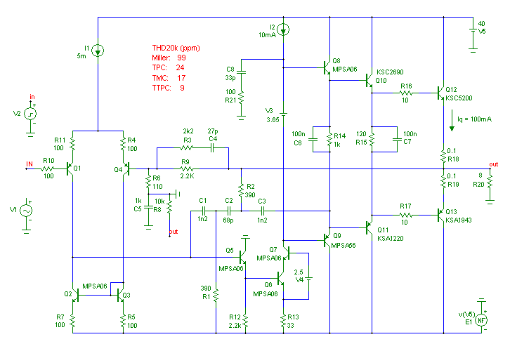
http://www.diyaudio.com/forums/soli...terview-negative-feedback-64.html#post2370317
C1 and R1 form a shunt compensation across the TIS input. Miller and shunt compensation together is a bad thing because shunt compensation lowers TIS input impedance. The VAS degeneration makes this much worse. I calculate that with the 1.2n/390R shunt the VAS has a current gain of no more than 10 above 580KHz! You are using shunt and miller compensation together and ultimately losing part of the benefit of TTPMC because the shunt compensation emulates TPSC without the extra pole.
The bottom of R1 should go to the emitter of Q5. At Q6 or Q7 emitters it will cause positive feedback. In any case the shunt effect across R1 will be decreased by about a factor of 10, so TIS virtual input impedance will increase by this factor as well. I think this will make TTPMC much more effective (crossing my fingers). Putting R12 across the BE of Q6 will also increase VAS gain and linearity.
It seems that one can use TTPMC and cancel all the poles using the feedback network, but it's slow and tedious and I get a phase margin of 39 degrees! I think I can probably get a better stability margin by reducing BW.
I imagine I would add a 3rd pole to TPC by using 3 caps in series for MC, then an R to ground from each junction. I'm sure I simulated this once but wasn't impressed. For one thing it would load the VAS more which is probably counterproductive.
I am trying to rig up a schematic that I can test all these schemes on, but ultimately there are changes that have to be made for each scheme. For instance TIS degeneration is needed for shunt compensation but causes problems with miller. If we were using spice-devices all the schemes could be compared with the same circuit but using real devices different schemes can be "biased" towards a topology.
- Home
- Amplifiers
- Solid State
- Bob Cordell's Power amplifier book