I have never tried any other simulator. Look at these messages in the yahoo group:
Yahoo! Groups
There is some flak going around about this "crappy free simulator" by highly skeptical people... It looks to me like people already are skeptical when they try it, and when it fails because of their misuse, that is enough to confirm their skepticism. I say: learn to use it right!!! (isn't this sort of like video game console wars?)
Many models out there are just CRAP. They don't model the actual device at all, often they are a copy of another, sometimes unrelated model, or they are just full of nonsense values. The AC parameters are usually not bad but the DC ones are off the wall. Some models will even make SPICE crash. I really don't get how manufacturers get away with the models, but they do. Fairchild ones are not as bad I've found.
Also, the models included by default with LTSpice are copies from other model libraries. I'm guessing they are included because the developers didn't find anything wrong with them.
I got the CCS to work for the VAS but when adding for the LTP, LTSpice has a total cow. It just won't converge. Screwed with the convergence settings and everything... So I'll give you this file with just the VAS replaced and working right.
I also added ESR to the filtering caps, to make PSRR realistic. Distortion has come to .002%, unless I screwed some adjustment up...
- keantoken
Attachments
I have never tried any other simulator. Look at these messages in the yahoo group:
Yahoo! Groups
There is some flak going around about this "crappy free simulator" by highly skeptical people... It looks to me like people already are skeptical when they try it, and when it fails because of their misuse, that is enough to confirm their skepticism. I say: learn to use it right!!! (isn't this sort of like video game console wars?)
Many models out there are just CRAP. They don't model the actual device at all, often they are a copy of another, sometimes unrelated model, or they are just full of nonsense values. The AC parameters are usually not bad but the DC ones are off the wall. Some models will even make SPICE crash. I really don't get how manufacturers get away with the models, but they do. Fairchild ones are not as bad I've found.
Also, the models included by default with LTSpice are copies from other model libraries. I'm guessing they are included because the developers didn't find anything wrong with them.
I got the CCS to work for the VAS but when adding for the LTP, LTSpice has a total cow. It just won't converge. Screwed with the convergence settings and everything... So I'll give you this file with just the VAS replaced and working right.
I also added ESR to the filtering caps, to make PSRR realistic. Distortion has come to .002%, unless I screwed some adjustment up...
- keantoken
Yes , you do have to know SOMETHING to make the best use of LT. Multisim is like a video game , all GUI and presets .. just your typical "Walmart simulator". I will try your sim and ""ferret" out any new tricks within. You are at present , in my opinion , the best "simulation jockey" on the site at the moment. This title was previously held by Andy C. , whom I thank for MY introduction to LT.
Using LT , then having the real thing to play with proves beyond a doubt that simulations are not "lies", as they are VERY close to real world operation.
OS
Okay, replace C6 with 5pF instead of 22p, and C7 with 680pF. Then make sure the line reads ".param dlycyc=1", I turned this off to find the oscillation. C7 prevents the CCS from oscillating.
Now THD reads less, at .0005%. I forgot I made those changes.
I would comment more, but don't have time at the moment.
- keantoken
Now THD reads less, at .0005%. I forgot I made those changes.
I would comment more, but don't have time at the moment.
- keantoken
I was never able to honestly compare, here is a file for full simulation of both versions. I was in a hurry before. Yes, there is barely a difference in distortion for this position. I think in the LTP the CCS would work better.
Some say a precisely matched LTP improves sonics audibly, and if this is true I wonder what effect the voodoo CCS will have.
I wasn't able to simulate the CCS for the LTP because the simulator won't converge (not soon at least)... It evidently has problems with this type of CCS. So I don't know how much gain there is by putting it there.
- keantoken
Attachments
Ah , you got it... keen. 6- 1 millionths of a mA , WOW. Must be voodoo. 
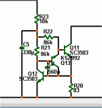
a ??? R21,22,20 custom values. Are these needed to make this thing stable ? By that huge 560pF cap at the base of Q13, it appears that there is a stability issue ??? And wahib's fourier shows very little improvement in performance. Hmmmm.
OS
a ???
R21,22,20 custom values. Are these needed to make this thing stable ? By that huge 560pF cap at the base of Q13, it appears that there is a stability issue ??? And wahib's fourier shows very little improvement in performance. Hmmmm.OS
Attachments
I wouldn't expect it to make any difference in the VAS position, but I would try it on the LTP.
The higher R22 and R21, the better performance, because the feedback loop has more to "kick against". I don't know if the bootstrap is necessary, I'll let you be the judge of that - the rail filtering probably works well enough. I chose the resistors to keep at least 1mA quiescent through Q13 and Q12. R22 current subtracts from output current.
- keantoken
Ostripper, when you run that wire, what node should the shield be connected to?
consider tapping the shield into the output. Then at the -IN end, the shield is at output voltage and the core is also at output voltage and so is not influenced by any other interference that passes close by.If you run the shielded wire just tack the ground shield to the voltage board ground connection on just 1 end of the wire . I did this on the first "frugalamp" (like the AX) no problems.
Connecting the feedback shield to any ground reference just seems wrong. But I'm no expert, on anything.
consider tapping the shield into the output. Then at the -IN end, the shield is at output voltage and the core is also at output voltage and so is not influenced by any other interference that passes close by.
Connecting the feedback shield to any ground reference just seems wrong. But I'm no expert, on anything.
Would that not be the same as a plain single core wire ??? You are very concise , Andrew.. don't sell yourself short. I would not want to have a "shootout" with you in the math classroom.
After further thinking , being of such a low impedance the output/NFB trace should not be affected by the rail current traces or capacitor returns until after it is dropped to a low level after the feedback resistor. This does not happen on this amp until the NFB is behind the VAS (in the realm of small signals).
OS
looks like I need to explain further.
A shield protects what is inside from outside influence. There are a couple of conditions (I think it was Conrad Hoffman that posted these).
cond1.) the shield must be very close to circular.
cond2.) the core must be very near the geometric centre of the shield.
In this situation any interference passing near the shielded core will be attenuated by the shield so the the core carries it's signal with little contamination.
Next the shield must be connected to a low impedance reference to conduct away the interference we are trying to avoid. Admittedly most situations use signal ground as the shield reference and often use the shield as the return route for the flow in the core.
But the output is also a low impedance reference. It will work just as well in shunting the interference that the shield is intercepting.
Why would a long wire not be good for taking an NFB signal from the output to the -IN terminal? Because it may pick up interference. How does it do that if it is connected to a low impedance reference? Because the inductance of the long wire raises the wire's impedance to HF and as the wire gets longer the inductance gets higher and the -IN end of the connection becomes more susceptible to picking up interference.
If the core is at the same potential as the shield then it cannot pick up interference from the shield, nor can it have parasitic capacitance to conduct a potential from shield to core, they are at the same voltage. If the shield is attenuating external interference then the core is carrying a less contaminated signal to the -IN end.
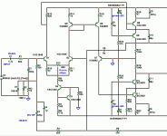
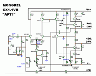
Next on the "chopping block" is a real classic. Called the "APT1" , it was designed in Cambridge ,Mass. by a Tomilson Holman. I had a chance to chat with the designer http://www.diyaudio.com/forums/solid-state/70261-apt-1-power-amp-undeservedly-forgotten-8.html when I was "green" (still am). He said " but I don't think it can be reproduced today since some of transistor types are no longer made."
HA HA , eat your heart out.... (BELOW) I am VERY pleased with this one as it spec'ed out to the original's performance BEFORE the refinements. On "first click"
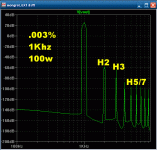
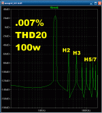
thd was .015% and even dropped to .01% at higher freq's - 20Khz/100w (strange). I then added a cascode under the level shifting current mirror to allow for the use of the KSA992, which is a much better device than the originals or the mpsa92 that I used before to handle the 150v rail to rail voltage requirement.These changes dropped the THD to .003% .. all the way to 10khz... and just slowly increasing to .0075% all the way up to over 30KHZ!
Same story at 200w , it "held" that same .003 to .007% all the way into the ultrasonics while also keeping the same H2 dominant harmonic distortion "signature". H5/7 were real low , as good as the AX (blameless).
Below is the GX. I am so impressed by it's harmonics that I might build this one for myself FIRST.
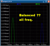
Another thing unique to this topology is that it seems to "force" a balance between LTP currents.. (last pix) at all power levels and frequencies, I attribute this to the use of the level shifting CM.
OS
HA HA , eat your heart out.... (BELOW) I am VERY pleased with this one as it spec'ed out to the original's performance BEFORE the refinements. On "first click"
thd was .015% and even dropped to .01% at higher freq's - 20Khz/100w (strange). I then added a cascode under the level shifting current mirror to allow for the use of the KSA992, which is a much better device than the originals or the mpsa92 that I used before to handle the 150v rail to rail voltage requirement.These changes dropped the THD to .003% .. all the way to 10khz... and just slowly increasing to .0075% all the way up to over 30KHZ!
Same story at 200w , it "held" that same .003 to .007% all the way into the ultrasonics while also keeping the same H2 dominant harmonic distortion "signature". H5/7 were real low , as good as the AX (blameless).
Below is the GX. I am so impressed by it's harmonics that I might build this one for myself FIRST.
Another thing unique to this topology is that it seems to "force" a balance between LTP currents.. (last pix) at all power levels and frequencies, I attribute this to the use of the level shifting CM.
OS
Attachments
looks like I need to explain further.
A shield protects what is inside from outside influence. There are a couple of conditions (I think it was Conrad Hoffman that posted these).
cond1.) the shield must be very close to circular.
cond2.) the core must be very near the geometric centre of the shield.
In this situation any interference passing near the shielded core will be attenuated by the shield so the the core carries it's signal with little contamination.
Next the shield must be connected to a low impedance reference to conduct away the interference we are trying to avoid. Admittedly most situations use signal ground as the shield reference and often use the shield as the return route for the flow in the core.
But the output is also a low impedance reference. It will work just as well in shunting the interference that the shield is intercepting.
Why would a long wire not be good for taking an NFB signal from the output to the -IN terminal? Because it may pick up interference. How does it do that if it is connected to a low impedance reference? Because the inductance of the long wire raises the wire's impedance to HF and as the wire gets longer the inductance gets higher and the -IN end of the connection becomes more susceptible to picking up interference.
If the core is at the same potential as the shield then it cannot pick up interference from the shield, nor can it have parasitic capacitance to conduct a potential from shield to core, they are at the same voltage. If the shield is attenuating external interference then the core is carrying a less contaminated signal to the -IN end.
I understand , It will be easy to implement as well.
OS
It's taken me a while to remember the name, but this is similar to "guard ring". This is a standard technique for sensitive inputs to remove or attenuate the effects of parasitics affecting the amplifier input.
It is that idea I'm trying to explain here.
I wonder if this guarding technique would be useful for all NFB traces. A pair of output connected traces laid one to each side, close to and parallel to the route all the way back to the -IN point would attenuate on PCB interference from affecting the NFB signal?
Discussion???
If there is a useful discussion to be had, then a new thread would be appropriate.
Last edited:
It's taken me a while to remember the name, but this is similar to "guard ring". This is a standard technique for sensitive inputs to remove or attenuate the effects of parasitics affecting the amplifier input.
It is that idea I'm trying to explain here.
I wonder if this guarding technique would be useful for all NFB traces. A pair of output connected traces laid one to each side, close to and parallel to the route all the way back to the -IN point would attenuate on PCB interference from affecting the NFB signal?
Discussion???
If there is a useful discussion to be had, then a new thread would be appropriate.
There is an excellant article about that here ...
Grounding Strategies for Printed Circuit Boards
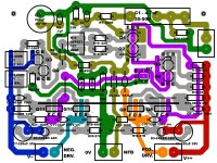
as you can see below , I already do the "guard ring" technique on my VB's(input section). BTW the "APT" GX1.1VB is DONE! Look for the errors.. Ha HA. Compare schema to layout , for this was done mentally , It COULD happen !!
OS
Attachments
Last edited:
Hi OS
I'm keen to build the PB60 with CX1, and have a few queries.
1) KSC3503 appears to come in different hFE values depending on the suffix letter, for example KSC3503D (hFE:60~120). Could you please confirm which variant to use? (or not matter)
2) I can't source Qnjw0302g/Qnjw0281g, but can source njw0302g/njw0281g. Likewise, I can't source Q2SA1837/Q2SC4793, but can source 2SA1837/2SC4793. Could you please confirm these are the same devices?
3) Could you please explain how to build the 3.3uH inductor (gauge/turns/diameter)?
4) I'm not familiar with getting PCB's professionally printed. Is it sufficient to simply submit your PCB jpeg and parts mirror jpeg?
I take it that the parts mirror is intended to be top-side?
and is it normal to submit the screen-print in a mirrored format?
5) I take it that the output and driver transistors protrude out beyond the PCB for mounting onto the heatsink (as per photo examples of your previous builds), but this creates a form-factor issue for people like me retro-fitting this into slimline cases/heatsinks (which I imagine would be typical for the PB60). My case is 80mm high with 75mm high heatsink, and your PCB is 76mm plus the height of the transistors, so it doesn't fit. I have a work-around but is a bit messy. Your original powerboard prototype would have been perfect. Anyway just a bit of "food for thought".
Thanks for your assistance, and I really appreciate you making this public domain for DIY'ers like me!
Craig
Hi OS
I'm keen to build the PB60 with CX1, and have a few queries.
1) KSC3503 appears to come in different hFE values depending on the suffix letter, for example KSC3503D (hFE:60~120). Could you please confirm which variant to use? (or not matter)
2) I can't source Qnjw0302g/Qnjw0281g, but can source njw0302g/njw0281g. Likewise, I can't source Q2SA1837/Q2SC4793, but can source 2SA1837/2SC4793. Could you please confirm these are the same devices?
3) Could you please explain how to build the 3.3uH inductor (gauge/turns/diameter)?
4) I'm not familiar with getting PCB's professionally printed. Is it sufficient to simply submit your PCB jpeg and parts mirror jpeg?
I take it that the parts mirror is intended to be top-side?
and is it normal to submit the screen-print in a mirrored format?
5) I take it that the output and driver transistors protrude out beyond the PCB for mounting onto the heatsink (as per photo examples of your previous builds), but this creates a form-factor issue for people like me retro-fitting this into slimline cases/heatsinks (which I imagine would be typical for the PB60). My case is 80mm high with 75mm high heatsink, and your PCB is 76mm plus the height of the transistors, so it doesn't fit. I have a work-around but is a bit messy. Your original powerboard prototype would have been perfect. Anyway just a bit of "food for thought".
Thanks for your assistance, and I really appreciate you making this public domain for DIY'ers like me!
Craig
1 - ksc3503/ksa1381 Hfe... classification E or F will be sufficient. I use the "E"
2 - The "Q" is a remnant from my simulator (I will correct that on schema) ,your assumptions are correct.
3 - Inductor - use 1/2" dowel or pencil , wrap 18 ga. magnet wire 15 turns one layer or 8 turns 2 layers. Mount 3W resistor (R98) on board first , then bend the wire on the outside of your new inductor into the inside of the 1/2' circle. Inductor mounts vertical on PB60 V1.1.
4 - About the PCB's , print them out on (staple's) photo paper , iron them on to your pcb material at high heat , soak in warm water , etch in peroxide/HCL (muriatic acid). they look as good as what a pro will do. I have never not made my own stuff , so I can't tell you. Mirrored image is top screen print.
5 - If you could hold on a few days I will make a PB60 "low profile" , I made these (PB60-250) for the standard 125mm (5") aftermarket heatsinks.
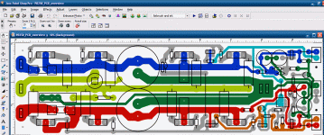
As far as boards ... I am going crazy with "Updates" 1/3 of amp performance is layout. The PCB/schema programs do not have all the "tricks" integrated into them.
The PB250 (Below- 1) - TONIGHT ..I will have an advanced version with Dr. jagodic's Cap multiplier , larger voltage board caps, LED'S
 better star grounding , AND the proper implementation of Doug self's magic Vbe resistor. NFB return will go shielded direct from inductor to euroblock.
PB60 - I did not change that. ALL is good.!!
NEW!!
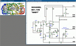
 BX1.1 (below-2) the "BaBy" smooth sounding classic RCA bootstrapped. amp..
 TO DO ... I will make the low profile board (will be the PB60LP) couple days.
FX - super pair amp
EX - "Leach amp" fully complimentary input stage with classic leach VAS.
OS
Attachments
Last edited:
- Status
- This old topic is closed. If you want to reopen this topic, contact a moderator using the "Report Post" button.
- Home
- Amplifiers
- Solid State
- The MONGREL (supersym II)