Ok I have a few designs I want you guys to look at , tell me if this could be potentially functionnal at making a sine wave , this is not for best audio quality possible remember .
I have this idea in mind , class b like with bias , using active rectifiers . What could be the downside of this , I need basicly a very fast settling , low offset op amp to minimize the noise .
Also I have this other idea in mind...
balanced/unbalanced preamplifier
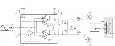
Could this drv134 make a functionnal phase splitter with biasing done this way ? Is this thing too unstable if both half circuits with are not exactly same impedance/resistance , these mosfets capacitance could vary and the transfo impedance as well ... ? I just want the voltage at the mosfet gate to the same basicly ... Personally I dont understand this circuit , It seems like it would be simpler to just use a regular op amp inverting and non inverting but I read this is no good ...
I have this idea in mind , class b like with bias , using active rectifiers . What could be the downside of this , I need basicly a very fast settling , low offset op amp to minimize the noise .
Also I have this other idea in mind...
balanced/unbalanced preamplifier
Could this drv134 make a functionnal phase splitter with biasing done this way ? Is this thing too unstable if both half circuits with are not exactly same impedance/resistance , these mosfets capacitance could vary and the transfo impedance as well ... ? I just want the voltage at the mosfet gate to the same basicly ... Personally I dont understand this circuit , It seems like it would be simpler to just use a regular op amp inverting and non inverting but I read this is no good ...
Attachments
It's best to start out with a clear objective, not just chuck a load of components together and then go: 'by Jove, you know I think that might produce a sinewave.' This is akin to designing by simulation, another technique which is definitely not recommended.
What exactly are you trying to achieve?
w
What exactly are you trying to achieve?
w
Thx for reponse
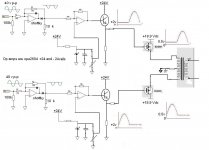
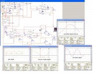
What I am trying to achieve is a half wave that is biased without going through a capacitor network wich totally distorts and allows for both mosfets to be biased seperatly since mostly likely my mosfets wont be prefectly matched, the npn common emitter at the end is to help with the capacitive loading and make this a real easy load for the op amp . How do people usually bias a half wave ? I dont like the kink and transcient created with class b when there is an inductive load .
I simed it on multisim and this gives a biased half wave rectified with no space in between both halves . Granted this was done with a virtual op amp , there is only the 741 with my multisim and that is not a modern op amp .
What about the drv134 , is this how it is usually biased ? Supposing my mosfets were closely matched for this design .
Last edited:
Ok so this might be bad , but your comments are not very constructive .
Wg_ski might I ask you what crossover distortion you are talking about ,the only non linear device here is the shottky diode . I am not gonna operate a 1.5 volt vgs device in a "cutoff method" , whatever that may be . I came here to try and learn and make my thing better not worse .
The thing that bothers me about this is that its big and expensive , the drv134 method is simpler and smaller ... but on the sim it is functionnal however and I doubt the crossover would be that bad with such a large signal , if you had very closely matched amps this would be good . The part that worries me is the falling edge of the half rectified wave inverting buffer , this was an oscillating in the sim when zooming in much , this might not finish smoothly , also biasing offset noise with the op amp . Utmost quality op amps could make this functionnal .
What could really help me , is if somebody could kindly educate as to how one should bias a circuit similar tio the drv134 so I can forget all about this whacky trash rectifier I made, could an adjustable power supply/low offset buffer be placed instead of the battery ?
thx you .
Last edited:
Personally I dont understand this circuit...
No, and none of the rest of us are going to understand it either, until you tell us what are the inputs and what outputs you want. This includes the frequencies, magnitudes and phase relationships if significant.
This is as constructive a reply as you are likely to get. Your posts are disorganised and it is almost impossible to plumb their meaning. No-one reading this is clairvoyant.
What I am trying to achieve is a half wave that is biased
What on earth does this mean?
w
What I am trying to achieve is a phase splitter , to run a mosfet type push pull source follower . Siignal will be a sine wave , in the audio ranges , at large signal levels 30 v-p-p or more . My ultimate goal is to have a sine wave on the output transformer secondary .
My quastion was , is this how you usually bias a differential phase splitter like the drv134 one , see the images .
I dont know how to make it more clear than this without boring you guys before you read the whole post .
My quastion was , is this how you usually bias a differential phase splitter like the drv134 one , see the images .
I dont know how to make it more clear than this without boring you guys before you read the whole post .
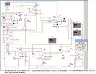
So I have simmed the drv circuit with regular op amps and coupling caps before the b+ in the middle , it seems to work like an phase splitting transformer .
What is the usual problem with this type of config , why does zeus amp use an transfo when they are big and expensive ?
I heard that both half circuit impedance must be exactly the same or "noise" is created , how is this ? I will never had the exactl same impedance w, theres gonna be mosfets there ( wich vary alot ) and a primary winding wich may or may not be perfectly symetric .
I believ I understand the basic of the drv134 circuit , basicly they are tracking one another to make sure they always have ther same amplitude but in opposite polarity . Where as a regular paraphase type op amp phase splitter ( very simple inverting and non-inverting with same exact gain ) just has the exact same gain with precision resistors and has no feedback between them to track eachother .
My question is basicly why not use regular paraphase if the differential type suffers from noise if impedance is not perfectly matched , where as regular paraphase just tracks the voltage at its output and doesnt give a damn after that what impedance its driving as long as its not strangely capacitive or too big a load for it , what is the point of the differential design , what are its advantages ?
thx you.
OK, it is entirely possible to produce an amplifier using a pair of non-complementary MOSFETs in a source-follower configuration.
Look at the sites of Susan Parker:
Audiophonics -
and John Broskie:
index
The circuit mimics a valve (tube) output circuit with the exception that the transformer is normally in the anode (would be the drain in this case) circuit with B+ connected to the centre tap. Valve circuits are arranged like this because there are no complementary valves.
Phase splitters can be problematic insofar as achieving good balance and accurate opposition, although this is less true in semiconductor circuits with multiple active devices in an IC.
It is simpler nevertheless to omit them from designs where possible.
Why would you want to employ a transformer when there are perfectly competent complementary MOSFETS available, capable of driving a speaker directly?
Some designers nevertheless feel that a limited number of components provides benefits which outweigh employing large numbers of components, regardless of cost or hand matching of components.
If you were to attempt to build a circuit of this general arrangement then the first requirement would probably be MOSFETs with matching characteristics. Some feature permitting independent adjustment of the bias in the 2 limbs of the circuit might be advisable.
The output of the phase splitter would probably benefit from buffering in order to reduce any variations due to loading, depending on the exact design. This might be achieved in a gain stage, however.
Lastly, in order to achieve the voltage swing you require, gain stages for each side will be required. At least one limb will probably require provision for adjustment of the gain in order to equalise it with the other.
A design like this requires detailed analysis and probably the construction of numerous prototypes. Exactly what biassing and how it is achieved is for you to decide once your circuit analysis capability has reached the point where you can evaluate the impact of the impedances of the components you decide to employ on the existing circuit and the likely outcome in terms of the distortion levels achieved.
w
Thx you wakibaki , is there a perfectly reliable and stable/cheap phase splitter out there thats made with op amps or is this one the way to go ? Is this one the way to go ?
http://www.diyaudio.com/forums/chip-amps/126529-balanced-unbalanced-preamplifier.html
http://www.diyaudio.com/forums/chip-amps/126529-balanced-unbalanced-preamplifier.html
Last edited:
check also out post #83 about
http://www.diyaudio.com/forums/soli...odels-quasi-complementary-power-output-9.html
http://www.diyaudio.com/forums/soli...odels-quasi-complementary-power-output-9.html
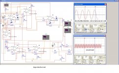
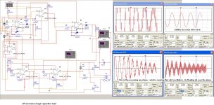
Here are some observations/simulatins from my design , I just wanna make an power amplifier that can handle reactive loads and stay sine , maybe with a little power with that , a capable sine wave oscillator if you will , for tesla experimets . So I am a bit going blind here since my load is a total mystery , I guess the transformer needs to be matched to the still undiscovered load , Or maybe I will go for a one size fits all impedance bridging transformer instead , is there such a thing as a low impedance transformer with Ok coupling factor ?
Anyways , these simulations are crap , there is no good transformer with center tap , all secondaries are messed up , its as if this was meant for tubes , I dont know much about these transformers . I am aware of the forumula for a voltage drop across a component is = current squares * impedance .
As you can see , my self-made circuit topology actually works , loves resonant loads and inductive loads , large capacitance not so good , still gives a tiny amplitude sine after a bit settling time , I guess the lower the secondary impedance the better it is for capacitive loads . It seems to be quite similar to the single ended in terms of various reactive loads besides the tiny little distortion , to me that is very acceptable . I think I will go with my design after all and start designing a pcb , I like the simplicity of it , I like the adjustable biasing on both legs , I like the direct coupling and the simple power supply . Modern op amps are good enough I think , I dont believe these people that say many active components = bad . I could are less about 1 % THD...
Here are some simulations , obervation , circuit waveforms . Might seem noobish but heh ... All these were taken at 20 khz
Comments are very welcomed , I think I have leveled up at DIY , you cannot ignore these noob posts anymore , for I have actually made my own working amplifier .
Attachments
Last edited:
Ok I will explain the thinking of this amp I made
When studying different designs , I relised that an transformer is an inductor , and inductors like continuous conduction of current ,otherwise they try to oppose with more voltagein reverse , this makes transcients that you must freewheel , this is bad for semidonductors but some can absord. I then realised that continous conduction is a must .
Then I said to myself , I must bias a half wave , thn this is the only way I could do it , I tried and tried... , does somebody have another topolology with semidonductors that can bias a half sine ?
Hi
A half wave rectified, sine wave signal is not (SIN X)/2 or (SIN X/2). It contains very high frequency components that are sure to get into and destroy your audio signal. Crossover distortion is similar and is a thorn in the side of most audio designers. I think you should forget the transformer if your intent is to build a SS amp. There is no good reason to use transformer signal coupling for solid state. If you intend to build a balanced amp (full bridge OPS) there are better phase splitting solutions out there. For example, THAT corp. has the 1646 SE to balanced converter IC. I use a descrete solution based on a bridge amplifier topology but it is not simple. However it works with perfect symetry >1MHz.
A half wave rectified, sine wave signal is not (SIN X)/2 or (SIN X/2). It contains very high frequency components that are sure to get into and destroy your audio signal. Crossover distortion is similar and is a thorn in the side of most audio designers. I think you should forget the transformer if your intent is to build a SS amp. There is no good reason to use transformer signal coupling for solid state. If you intend to build a balanced amp (full bridge OPS) there are better phase splitting solutions out there. For example, THAT corp. has the 1646 SE to balanced converter IC. I use a descrete solution based on a bridge amplifier topology but it is not simple. However it works with perfect symetry >1MHz.
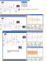
Isnt it the same thing as class b push pull transformer coupled ?
Class b uses half-wave rectified only it has crossover distortion , this is what used to be used in am radio .
This to my opinion is the same exact thing only better , if the op amp doesnt screw up this should work .
I tried different capacitive loads with a pure class a zeus type and the same thing with my own design .
They react exactly the same when the same transformer is used , if one shows massive distortion with a large capacitive load so those the other , and so does single ended.
For every single load I test it all reacts the exact same wayminus the small distortion either my design or zeus or single ended , big inductors , small caps , big caps , semi resonant , full resonant whatever ...
http://www.diyaudio.com/forums/solid-state/169051-functionnal.html
Last edited:
- Status
- This old topic is closed. If you want to reopen this topic, contact a moderator using the "Report Post" button.
- Home
- Amplifiers
- Solid State
- Could this ever be functionnal