I just picked up a couple of cheap assembled amplifier PCB's from a Chinese seller on Ebay.
I've got them all connected up properly, however I have approx 2 volts DC on the output even when the offset potentiometer (W2) is adjusted all the way to the end, and the input is grounded.
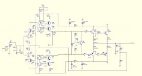
I though that maybe some of the resistors values might have been substituted at assembly, but all appears correct when compared to the schematic.
I know that I could probably fiddle it by changing resistors LR8 and LR25 for something bigger, but i'd rather know what's actually the problem.
Can anybody spot any obvious mistakes on the schematic? Any ideas what could be causing this?
I've got them all connected up properly, however I have approx 2 volts DC on the output even when the offset potentiometer (W2) is adjusted all the way to the end, and the input is grounded.
I though that maybe some of the resistors values might have been substituted at assembly, but all appears correct when compared to the schematic.
I know that I could probably fiddle it by changing resistors LR8 and LR25 for something bigger, but i'd rather know what's actually the problem.
Can anybody spot any obvious mistakes on the schematic? Any ideas what could be causing this?
Attachments
That might explain a few things... In theory, they should be matched, but I doubt they actually are. Where would I obtain matched 2SK170BL and 2SJ74BL pairs?
If I install a 220 ohm resistor in place of LR8 and do away with LR25 and W2, and install a trimmer in place of LR3 and LR4, should that do the trick?
If I install a 220 ohm resistor in place of LR8 and do away with LR25 and W2, and install a trimmer in place of LR3 and LR4, should that do the trick?
Hi
I would try a trimmer in place of LR3 to remove dc from the input and also a trimmer instead of LR8 to remove dc from that stage also. However it should be enough to just put a trimmer in place of LR8. I am assuming that you are finally adjusting when the amplifier is at running temperature.
Don
I would try a trimmer in place of LR3 to remove dc from the input and also a trimmer instead of LR8 to remove dc from that stage also. However it should be enough to just put a trimmer in place of LR8. I am assuming that you are finally adjusting when the amplifier is at running temperature.
Don
Here, http://www.diyaudio.com/forums/swap-meet/161366-matched-toshiba-fets-sale.html
Not cheap but much more reliable and without risk factor.
Not cheap but much more reliable and without risk factor.
reminds of terrible elektor designs that are simulation products and mostly based on perfect parts that actually dont exist ....
the construction /time/effort /cost/ consumed to pick up the proper parts might be twice as much than the cost of amplifier it shelf .... Titan i thing the miracle was called ...
i will go though with amv8 and see where is this 2 volt originate from ...
the construction /time/effort /cost/ consumed to pick up the proper parts might be twice as much than the cost of amplifier it shelf .... Titan i thing the miracle was called ...
i will go though with amv8 and see where is this 2 volt originate from ...
Hi Ben
i think i can help you because i have made twice the TITAN 2000 and CRESCENDO 2000
and input stage topology nearly matched
YOU MUST MATCH LT1 - LT2 if you don't matched you can't never take 0V Offset
i post my result about TITAN 2000 ON POST 59 ----LEGEND sTAGE MK2 IN MAKING............ SOLID STAGE PAGE 4 NOW
Hi,
Thanks once again for the helpful suggestions. I've done some more measuring, and indeed, the two input Jfets are nowhere near matched. I tweaked the value of LR8 just to get the amplifier in a working state.
I'll have a look at the thread that Homemodder suggested, and try to purchase some matched Jfets for this.
What makes these amps "current mode?"
I think it's a current feedback design, because the current to charge/discharge LC2 is provided via the two current mirrors by LT1 and LT2, and so by the signal on the inverting input (the common point of the source resistors of the jfets). However, the source resistors are somewhat high in value, so the feedback network's impedance into the inverting input will only have a limited influence on the location of the dominant pole once its impedance gets lowish (as it is now). It will however make the amplifier slower once its impedance gets significantly above 60 Ohms.
reminds of terrible elektor designs that are simulation products and mostly based on perfect parts that actually dont exist ....
the construction /time/effort /cost/ consumed to pick up the proper parts might be twice as much than the cost of amplifier it shelf .... Titan i thing the miracle was called ...
i will go though with amv8 and see where is this 2 volt originate from ...
It will work quite happily but with reduced performance without matched parts provided you trim the offset the way I discribed.
Although this amp vas is different to what I use I wouldnt call it a simulation product, Im not 100 percent sure but this type design has been in use for some 30 years. Is it worth time, effort, cost, my answer is absolutely yes, designed and built properly it simply sounds better than any Self type amp and much better than a P3 amp, its simply in a diffirent legue.
I think it's a current feedback design, because the current to charge/discharge LC2 is provided via the two current mirrors by LT1 and LT2, and so by the signal on the inverting input (the common point of the source resistors of the jfets). However, the source resistors are somewhat high in value, so the feedback network's impedance into the inverting input will only have a limited influence on the location of the dominant pole once its impedance gets lowish (as it is now). It will however make the amplifier slower once its impedance gets significantly above 60 Ohms.
I guess I'm a bit thick. It still looks like the feedback signal is derived by dividing down the output voltage and applying that to the inverting input. LC2 is only 45pF so would appear to be compensation. So it still looks to me like a conventional constant-voltage amplifier with voltage feedback.
the feedback signal is derived by dividing down the output voltage and applying that to the inverting input
A current feedback amplifier has that too. Only, the impedance provided at the - input determines how fast the amplifier will settle because the current into the inverting input is passed onto Cdom. Low impedance = fast settling but reduced phase margin. So with low gain you provide a high(ish) impedance to get the amp stable, while at high gain, the impedance of the feedback network can be lowered because the increased gain margin allows you to do so. As a result, a high gain configuration can be as fast as a low gain config. Voltage feedback amps cannot do this.
Last edited:
OK, you'll have to go a little slower for me. I get that when they say "current mode," they don't mean "constant current" amplification in the Mills & Hawksford sense. But looking at the feedback, the capacitor is across a 47k resistor. That's an f3 of 80kHz- I can't imagine that, in most of the audio band, there's any significant effect of the cap, and the feedback looks like plain vanilla voltage feedback. The cap appears to me to be a way of slowing down the NPN half to match the PNP half.
Sorry to be a pain, but I'm trying to understand this.
Sorry to be a pain, but I'm trying to understand this.
Yeah, but C0 effectively shorts the bases of the NPN and PNP drivers for any highish frequency. So LC2 is essentially parallel to both. If it really is compensation, then the designer is relying in the ESL of C0. Bad practice.
The design is a little strange (didn't look at the values), but the fact remains that the current into the - input matters, its impedance is pretty low and effectively in parallel with RF2. The current mirror is set to a ratio of about 4.8, so the current injected into the - input will be sent through LR12, LR14 (which are in parallel for this current path) and LC2 multiplied by 4.8. I guess that is whay they mean by "current mode". Altering the impedance of the feedback network would probably show a bit of shifting of the pole by LC2, but I don't know how much and currently I'm too lazy to grab a calculator.
The design is a little strange (didn't look at the values), but the fact remains that the current into the - input matters, its impedance is pretty low and effectively in parallel with RF2. The current mirror is set to a ratio of about 4.8, so the current injected into the - input will be sent through LR12, LR14 (which are in parallel for this current path) and LC2 multiplied by 4.8. I guess that is whay they mean by "current mode". Altering the impedance of the feedback network would probably show a bit of shifting of the pole by LC2, but I don't know how much and currently I'm too lazy to grab a calculator.
Sorry to be a pain, but I'm trying to understand this.
Have a squint at figure 1 in this AD appnote - the amp here is a variant of the Alexander Current Feedback amp : ADI AN-211. The main difference is here we have a complementary pair of JFETs acting as the input buffer in lieu of an opamp.
Mark Alexander also explains how the output offset arises and shows how to fix it with a servo amp.
- Status
- This old topic is closed. If you want to reopen this topic, contact a moderator using the "Report Post" button.
- Home
- Amplifiers
- Solid State
- DC on output of Chinese 'current mode' ebay amplifier