>You can also see the square wave output is higher at 1MHz than the sine wave at 1MHz (why is that? output transistor input capacitance? diff amp capacitance?)
The fundamental sine of a square wave is 4/pi times higher, see: Square wave signals : MIXED-FREQUENCY AC SIGNALS
I will answer the other questions later. Sorry, I have to go now.
edit: I'm back as there's a strike going on in Amsterdam.
Cheers,
E.
The fundamental sine of a square wave is 4/pi times higher, see: Square wave signals : MIXED-FREQUENCY AC SIGNALS
I will answer the other questions later. Sorry, I have to go now.
edit: I'm back as there's a strike going on in Amsterdam.
Cheers,
E.
Last edited:
using the scope pic showing ~8mVpp of noise and applying that to the noise prediction of the sim @ 0.167mVac, then the ratio of the two figures is ~50, rather than the >=3 that you mentioned.Below you see a sim of the output noise as function of BW. Up to 1MHz the noise is 167uV RMS. The peak to peak value is of course much higher, at least three times, depending on the crest value.
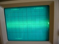
Also have a look at the output of one of my own amps. The noise is mainly dominated by HF ingress (Y=2mV/div, X=0.5us/div, BW=1MHz)
When I look at my scope output with the bandwidth reduced 20MHz (it's the only filter available to me) I usually see 2mVpp to 5mVpp as typical wideband noise.
thanks for the picture as it pleases me to see the trace is nearly identical.
I made a picture myself too. Check it out.
But I need to say, this is done with grounded input. If I leave the input flying or if I connect it to the generator (even if switched off) the figure is roughly 10x worse. In the case of a flying input there is 600KHz signal prominently apparant.
In the case (picture) of a grounded input there is a sum of 2 thing. An amount of 600KHz signal and another amount of around 30MHz signal.
There is always a very weak amount of 50Hz too. Not really as a signal but more like repetitive small spikes. I gues it's some battery charger or so...
Cheers,
Olivier
Attachments
HF ingress used as the descriptor rather than output noise from the amplifier?>then the ratio of the two figures is ~50, rather than the >=3 that you mentioned.
Of course the ratio seems much higher because the picture is highly distorted by HF ingress.
What is the difference when we are looking for the quietest output that the circuit is capable of?
The difference is that we are talking about two different noise sources: one that is generated by the amp itself and the other picked up by an unshielded speaker cable (or whatever) from outside noise sources. I'm afraid I'm missing your point.
edit: the reason I've included a scope picture is to make clear that without rigorous precautions the noise floor is always blurred by external sources and to make clear that Olivier's 2mV noise is nothing to worry about.
edit: the reason I've included a scope picture is to make clear that without rigorous precautions the noise floor is always blurred by external sources and to make clear that Olivier's 2mV noise is nothing to worry about.
Last edited:
Hi Edmond,
I am still not through your last postings about the OPS.
One thing on your schematic for the Front End : you changed the value of R16 & R17 to 100 Ohms. On the PCB actually they are bridged 0 ohms. I did that because I had oscillations on that node (both). However they were 1K resistors. Is 100E the best in between? How can this resistor cause oscillations anyway? It's a base resistor for the regulator Q, nothing more.
Hi Olivier,
I put there 100 Ohms, because I thought you didn't like empty spaces.
") The actual value is absolutely not critical, though the lower the better.
The actual value is absolutely not critical, though the lower the better.With 1k it oscillates? Measured with a 1:1 probe? If so, that means trouble. Always use a 10:1 attenuator probe.
Hereby some pictures of the actual situation.
First the PCB itself. You can use it to see what components are in place, not placed and what components are placed on the fly (temporary placement). You see the simple miller caps flying there, bridging from R43 to R36 and R44 to R37. You can also see the different ground nodes (Signal Ground (the one on the full left upper screw), the feedback ground (top screw, middle terminal block), the common ground (CGND see silkscreen), Decoupling Ground (middle screw, right terminal block, green wire). As you notice very few capacitors are installed : only input DC blocking caps (C2A & C2B), 1 pair of decoupling caps C3 & C4 (the larger decoupling electrolyts are not installed C11 & C10), The lead-lag caps C12/13, the CMCL caps C15/16, and finally C8 the small cap across the Feedback cap C7 which is also installed). Not installed are : The right hand side decoupling caps (electrolyt C26/27 + polyprops C24/25) as stated before the left hand side decoupling electrolyt caps C10/11, the bias filter cap CB, the cascode zener voltage ref filter caps C22/23, the TMC caps C18->21), C17A&B (added at the last moment they are for stability but don't know how yet), C5/6 the stability caps at the right leg of the diff amps. Also C9/R19 feed forward is not installed. Also different protection components are not installed (diodes, resistors). The only protection installed are the VAS current limiter Q's.
Long story but hopefully means something to you.
Other pictures are :
100KHz sine response
100KHz square response (the bottom overshoot is difficult to see but OK I read that is acceptable)
1MHz sine response
1MHz square response
You can see it is very near the ULGF -3dB point of the amplifier.
You can also see the square wave output is higher at 1MHz than the sine wave at 1MHz (why is that? output transistor input capacitance? diff amp capacitance?)
Also notice signal generator has some ringing on the square wave.
These pictures look okay. Probably, the ringing is caused by the cabling. Both ends of a coax cable should be correctly terminated (e.g. with 50 Ohms) to get a clean square wave.
Amp coops well with that I seem to believe. But is the generator supposed to do that? Bad generator or input of amplifier does this ?
Try to connect the generator to the scope with the shortest cable you have or otherwise with a well terminated coax cable. Now the ringing should be gone.
One more thing about your OPS. Do you think Error Correction is on the order for this amplifier?
Hmm... not now I would say. Perhaps something for a next project. TMC is almost as good as HEC . On the other hand, HEC needs more voltage swing from the VAS. That means a boosted PSU for the front-end (and most likely more modifications).
(I hope it is not incorporated in your OPS yet as I would deserve a slap in the face ).
No, it isn't. BTW, the OPS I've shown, is certainly not the final version. The only reason I've added it to the front-end is to observe the influence on the Miller loop response (and also to get an impression of THD figures).
Regarding the choice of output devices, both verticals and laterals have their pros and cons. Verticals can deliver more power, but need beefier drivers, gate protection Zeners and temperature compensation.
Of course it's up to you which one you prefer and (of course) which one you can get. The best verticals for audio are 2SJ201 and 2SK1530. Regrettably, it is said that Toshiba has discontinued the production of 2SK1530.
Cheers,
E.
thanks for the picture as it pleases me to see the trace is nearly identical.
I made a picture myself too. Check it out.
But I need to say, this is done with grounded input. If I leave the input flying or if I connect it to the generator (even if switched off) the figure is roughly 10x worse. In the case of a flying input there is 600KHz signal prominently apparent.
In the case (picture) of a grounded input there is a sum of 2 thing. An amount of 600KHz signal and another amount of around 30MHz signal.
There is always a very weak amount of 50Hz too. Not really as a signal but more like repetitive small spikes. I guess it's some battery charger or so...
Cheers,
Olivier
Hi Olivier,
In order to measure the real noise (and no rubbish from broadcast stations) you must shield everything, also the PCB.
(and ground the input)
Good luck.
E.
Good evening Edmond,
I have noticed some other changes in the schematic. Could you tell me why the change is made?
1) the diodes in the diff amp, right legs, are replaced by zener diodes D3/4 value 4V7?
2) The resistors in the current source legs are replaced by zeners D5/6 value 4V7 (you already mentioned this change)?
3) The feedback capacitor had a parallel leg which included a polypropylen capacitor. Is it useless or just deleted for simulation purpose?
4) The sequence of connection to the rails of the decoupling capacitor is particular. Is that how it should be intended on the PCB too? First it is placed between the VAS and IPS. Second, the RC filter between VAS and IPS is right in between both decoupling capacitors (the electrolyt C12 and the non polarized smaller one C8).
5) The non polarized caps are 10 fold larger. Is this really better?
6) C6 and C7 are of different value? I suppose it's a copy paste error.
7) Q21 and Q22 are 2N5551 & 2N5401 Q's whereas it was 2SC3503 and 2SA1381. In my circuit the developped power is very limit. In yours the power is lower. Why lower? Better lower?
8) Zeners D11 & D12 are changed from 6V2 to 4V7 equal to the cascode zeners. I made them slightly higher in order to be sure the cascodes cannot saturate. Is that wrong thinking then?
9) C17 A & B are removed. Are they useless?
I suppose we could replace all or most zeners by voltage references?
As for the OPS devices lets keep them Laterals 1058/162. The only bummer is the voltage limit 160V :-(
I will also look for higher voltage devices.
By the way what do you think of IRFP9240? Is vertical mosfet.
Cheers
Olivier
Hi Olivier,
Answering all these questions is a long story. May I propose to do this later?
First thing first and that is simulating the Miller loop response in a correct way.
edit: This has to done right, otherwise it makes no sense to go any further (see post 373).
Cheers,
E.
Answering all these questions is a long story. May I propose to do this later?
First thing first and that is simulating the Miller loop response in a correct way.
edit: This has to done right, otherwise it makes no sense to go any further (see post 373).
Cheers,
E.
Last edited:
Edmond,
What about this device?
Lateral Mosfet
VDS : 200V
Is there a drawback in this component? Besides price I suppose and probably sourcing?
Cheers,
Olivier
Looks nice !
Hi again,
They are available at RS components belgium for 11.54€/pc (in stock). The 160V version.
I also like this one :
ALF16N20W for 10.86€ sadly the P channel is unavailable.
ALF08P20W for 6.59€
ALF08N20W for 6.59€
There is no rush in answering any questions. I respect all the time want to spend.
I will simulate the miller loop according to the components on the actual pcb and will come back to you with results. I will try again with my own circuit and if the result is still strange I will adapt your schematic file to the actual components. Maybe I'll do the latter first as it might be faster
Cheers,
Olivier
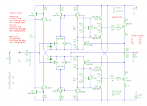
Class-I
Sorry, NOT that nice because of a common source connection. So you cannot insert source series resistors.
Regarding the other laterals, I would wait to purchase them, as it not impossible that the specific advantages of verticals outweigh the virtues of laterals.
The point is that someone kindly provided me a glimps into Kendall Castor-Perry's Class-I output stage, that is, a very basic sketch. So I don't know any details, but you can find it here: Linear Audio | your tech audio resource
In the meantime I figured out how his circuit might work and I must say (if my implementation is correct) that Kendall is really a genius. His circuit works even better than my autobias-II thingy: more tolerant to component mismatches and Iq is less temperature dependent (0.1%/K versus 0.3%/K). Brilliant! Chapeau!
Below you see a relative low power version with only one pair of vertical MOSFETs. The performance with laterals was less favorable, due to the extreme low Vgth and (probably) lower transconductance.
Notice that the use of separate push-pull drivers is an absolute necessity, as you can't use a single PNP-NPN EF stage with the ubiquitous speed-up cap between the emitters. Such a cap destroys the whole concept. Deleting the cap isn't an option either, as this will provoke cross-conduction.
Also notice the frequency compensation: C3, R8, C4 & R9. I don't know if Kendall did it the same way, but I think this is the only correct method (i.e. feed-through compensation)
Please have a look at it and/or run a sim. THD20 is really low: ~67ppm.
(but first the Miller loop, of course)
Cheers,
E.
Edmond,
What about this device?
Lateral Mosfet
VDS : 200V
Is there a drawback in this component? Besides price I suppose and probably sourcing?
Cheers,
Olivier
Sorry, NOT that nice because of a common source connection. So you cannot insert source series resistors.
Regarding the other laterals, I would wait to purchase them, as it not impossible that the specific advantages of verticals outweigh the virtues of laterals.
The point is that someone kindly provided me a glimps into Kendall Castor-Perry's Class-I output stage, that is, a very basic sketch. So I don't know any details, but you can find it here: Linear Audio | your tech audio resource
In the meantime I figured out how his circuit might work and I must say (if my implementation is correct) that Kendall is really a genius. His circuit works even better than my autobias-II thingy: more tolerant to component mismatches and Iq is less temperature dependent (0.1%/K versus 0.3%/K). Brilliant! Chapeau!
Below you see a relative low power version with only one pair of vertical MOSFETs. The performance with laterals was less favorable, due to the extreme low Vgth and (probably) lower transconductance.
Notice that the use of separate push-pull drivers is an absolute necessity, as you can't use a single PNP-NPN EF stage with the ubiquitous speed-up cap between the emitters. Such a cap destroys the whole concept. Deleting the cap isn't an option either, as this will provoke cross-conduction.
Also notice the frequency compensation: C3, R8, C4 & R9. I don't know if Kendall did it the same way, but I think this is the only correct method (i.e. feed-through compensation)
Please have a look at it and/or run a sim. THD20 is really low: ~67ppm.
(but first the Miller loop, of course
)Cheers,
E.
Attachments
Last edited:
Class-I
Hi Damir,
Maybe you have overlooked it, but the most important key figures are mentioned in the schematic (red text). I a couple of days I hope to give some more information in a separate thread.
To all,
Does anyone have the original article from Kendall? I don't have a copy. Much obliged if someone would send me a (scanned ) copy.
Cheers,
E.
Hi Edmond,
I still cannot figure out why my circuit does not show a correct millerloop response!?
I will continue to check.
However I stepped to your circuit for comparison.
I have a question anyway : the ML response around 200KHz shows a phase margin much lower than 90°. More like 40° ... is that a problem? What does affect the Phase in this circuit? Can it be optimized?
Cheers
Olivier
- Status
- This old topic is closed. If you want to reopen this topic, contact a moderator using the "Report Post" button.
- Home
- Amplifiers
- Solid State
- HEEEELLLPPP : M. Randy Slone Mirror Image Topology Construction - Troubles