Hi Edmond,
First of all, good thing to proceed in this thread as it is not longer directly linked to Bob's book thread.
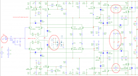
This is indeed the latest version of the schematic and pcb. It corresponds to the actual fabricated PCB. I have 3 copies (if you would be interested you can have one)
The OPS isn't even designed. Well there were some simulated attemps but since I struggled so much with the frontend I decided not to invest time in ops'es yet. This week-end I will do some more testing to see if this frontend is realy as solid as it seems. Then, the time has come for the OPS to be designed.
The railvoltage can be set at any voltage , however my goal is to achieve something like 250W into 8 ohms. Only my FET Vgd's are on the low side 160V (if I remember well - got only 6 of each so i can still switch to another device ...)
You also asked me the question if I would prefer stability for thd? Yes, part of the goal is to have a highly reliable and forgiving amp without going over 0.001% THD 20KHz 250W 8ohm BW till 10th harmonic. I don't know if this is possible.
Later on it needs multiple security circuitry which I would like to elaborate.
If you allow me some dreaming, I dream of an amplifier solid as a tank (power wise & reliability wise), with very very respectable thd+n, sober casing, and possibly a nice looking pcb design.
Back with my feet on the ground I will continue VAS testing and simulating the loop assessments. I also want to measue some parameters like 3dB roll-off points, phase lag, amplitude, maybe some other and compare them with the simulation. This should show how the real thing deviates from the simulation.
In my last pcb I had a serious problem of phase lag (see older posts) I think this time it's different.
I will also send a sketch of how my testlab is grounded and how the amp is wired to all that. It's now installed with best results (after trying and trying) but i believe it's rather luck and that the best solution on paper is not working as well in my case ... more about that later ...
Cheers,
Olivier
First of all, good thing to proceed in this thread as it is not longer directly linked to Bob's book thread.
This is indeed the latest version of the schematic and pcb. It corresponds to the actual fabricated PCB. I have 3 copies (if you would be interested you can have one)
The OPS isn't even designed. Well there were some simulated attemps but since I struggled so much with the frontend I decided not to invest time in ops'es yet. This week-end I will do some more testing to see if this frontend is realy as solid as it seems. Then, the time has come for the OPS to be designed.
The railvoltage can be set at any voltage , however my goal is to achieve something like 250W into 8 ohms. Only my FET Vgd's are on the low side 160V (if I remember well - got only 6 of each so i can still switch to another device ...)
You also asked me the question if I would prefer stability for thd? Yes, part of the goal is to have a highly reliable and forgiving amp without going over 0.001% THD 20KHz 250W 8ohm BW till 10th harmonic. I don't know if this is possible.
Later on it needs multiple security circuitry which I would like to elaborate.
If you allow me some dreaming, I dream of an amplifier solid as a tank (power wise & reliability wise), with very very respectable thd+n, sober casing, and possibly a nice looking pcb design.
Back with my feet on the ground I will continue VAS testing and simulating the loop assessments. I also want to measue some parameters like 3dB roll-off points, phase lag, amplitude, maybe some other and compare them with the simulation. This should show how the real thing deviates from the simulation.
In my last pcb I had a serious problem of phase lag (see older posts) I think this time it's different.
I will also send a sketch of how my testlab is grounded and how the amp is wired to all that. It's now installed with best results (after trying and trying) but i believe it's rather luck and that the best solution on paper is not working as well in my case ... more about that later ...
Cheers,
Olivier
LineSource,
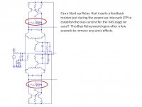
This type of circuit corresponds to Bob's method to tame the VAS fighting current issue. There are people here that can answer more accurately than me but I would say (cfr Bob's book) the helper Q helps eliminate or reduce Hfe difference between Q's. This help the VAS to fight less. The resistor across the IPS legs resolves the rest of the problem but in your case you will remove this resistor after startup? I suppose to get rid of its effect on loop gain? I guess you imagine this fighting issue is especialy there on the startup and that after settlement it can be removed. Like a starter in a neon lamp. I guess the circuit will still alter due to temperature effects and others.
Don't know if you tried yet : simulate your schematic. Remember the VAS current and change one of the Re resistors of the current mirror Q's by 1% up and 1% down. See what the VAS current does?
Cheers,
Olivier
Hi Olivier,
> I have 3 copies (if you would be interested you can have one)
You better keep them yourself. A spare PCB is always handy (for testing purposes etc) and use the other two for your final version.
>You also asked me the question if I would prefer stability for thd? Yes, part of the goal is to have a highly reliable and forgiving amp without going over 0.001% THD 20KHz 250W 8ohm BW till 10th harmonic. I don't know if this is possible.
I think 0.001% THD 20KHz is feasible, but not at 250W with only three pairs of lateral MOSFETs. The PGP amp has them too and syn08 wasn't happy with it (see the PGP website). Also I think that 75V is too high for these devices. I wouldn't go beyond 60V.
In the meantime, I'm experiencing troubles with the MOSFET models: MC 9 and MC10 give different results for the Vgs @ Id=150mA & Vds=63V
I've tested three pair of models:
1. Yours (form Hitachi?)
2. From the MC9 library
3. From this forum ( http://www.diyaudio.com/forums/parts/3230-p-spice-models-4-2sk1058-2sj162.html#post998418 )
Here are the results (Vgs in mV for N-channel respectively P-channel devices):
As you see, different and/or unrealistic results between MC9 and MC10. The only models that gave (almost) identical results are from this forum. So I'm inclined to use these ones. However, about -156mV for the 2SJ162 seems too low (err... I mean too high). To go any further with he sims I really need the correct Vgs as it might have a significant impact on the driver configuration (if Vgs-N - Vgs-P < 2*Vbe I need a different driver than in the case if Vgs-N - Vgs-P > 2*Vbe ).
So please would you be so kind to measure the real Vgs @ 150mA. No need to measure it at Vds= 63V. 10 Volts or so will do, otherwise the MOSFEts get too hot.
Cheers,
E.
> I have 3 copies (if you would be interested you can have one)
You better keep them yourself. A spare PCB is always handy (for testing purposes etc) and use the other two for your final version.
>You also asked me the question if I would prefer stability for thd? Yes, part of the goal is to have a highly reliable and forgiving amp without going over 0.001% THD 20KHz 250W 8ohm BW till 10th harmonic. I don't know if this is possible.
I think 0.001% THD 20KHz is feasible, but not at 250W with only three pairs of lateral MOSFETs. The PGP amp has them too and syn08 wasn't happy with it (see the PGP website). Also I think that 75V is too high for these devices. I wouldn't go beyond 60V.
In the meantime, I'm experiencing troubles with the MOSFET models: MC 9 and MC10 give different results for the Vgs @ Id=150mA & Vds=63V
I've tested three pair of models:
1. Yours (form Hitachi?)
2. From the MC9 library
3. From this forum ( http://www.diyaudio.com/forums/parts/3230-p-spice-models-4-2sk1058-2sj162.html#post998418 )
Here are the results (Vgs in mV for N-channel respectively P-channel devices):
Code:
model  MC9: Vgs-N  Vgs-P |  MC10: Vgs-N  Vgs-P
  1         +923   +250  |        +1186   -418
  2         +434    +26  |         +469   -373
3 +524 -154 | +527 -158So please would you be so kind to measure the real Vgs @ 150mA. No need to measure it at Vds= 63V. 10 Volts or so will do, otherwise the MOSFEts get too hot.
Cheers,
E.
Hi Edmond,
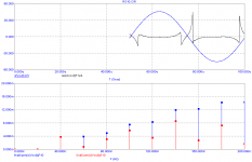
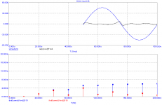
I simulated (MC9) the miller loop response according to your instructions. The components on the board show following simulation results : ULGF 32MHz with 85° phase margin. Gain margin is 22dB at 300MHz.
However in your picture the gain rolls of near lower frequencies whereas in mine it becomes flat at around 200KHz and less.
I will also try the same for the CMCL loop.
Tomorrow I will measure the Vgs of my fet devices.
But if you feel this devices are not suitable for me, I can change to another device ... I know you favor verticals right? That's also good for me, however laterals are very rugged.
Indeed the files cannot be opened within MC9.
About the rail voltage you are indeed right. 75V is limit limit. That might be an input to switch device.
About the amount of pcb's I have (3pcs) I will not use them in the final project as they are lacking things like : fusing, relays, the real ops or better no ops if front only (the ops is dummy and incorporated on this pcb). If the track layout is good i will keep most of it but it will be placed on a new board anyway.
I will come back to you tomorrow.
Cheers,
Olivier
Edmond,
I read about your PGP amp. The THD requirements you have there are 10 fold better than what I intend.
However the Q count in the PGP is really huge.
For my information, the principle or basic schematic of the PGP is far superior compared to the one I try to run? I ask this because I thought this amp is already very complicated. I mean the frontend (as the OPS is not designed yet)?
Cheers
Olivier
Edmond,
CMCL results (same circuit actual on the pcb) :
CMCL ULGF : 390KHz phase margin : 90 degrees
Gain margin 32dB at 30MHz
question : are one of the results of the cmcl and miller loop to be compared? I see the 0dB passage of the CMCL @ 30MHz which is near the ULGF of the miller loop ? Hazard or is there a link somehow?
Cheers
Olivier
Hi Edmond,
I simulated (MC9) the miller loop response according to your instructions. The components on the board show following simulation results : ULGF 32MHz with 85° phase margin. Gain margin is 22dB at 300MHz.
However in your picture the gain rolls of near lower frequencies whereas in mine it becomes flat at around 200KHz and less.
Hi Olivier,
Hmm... weird. Can you show a picture (and schematic)?
I will also try the same for the CMCL loop.
Tomorrow I will measure the Vgs of my fet devices.
Please.
But if you feel this devices are not suitable for me, I can change to another device ... I know you favor verticals right? That's also good for me, however laterals are very rugged.
Indeed, they are very rugged. So just keep them. Maybe you can get some more them, i.e. four pairs per OPS.
Indeed the files cannot be opened within MC9.
About the rail voltage you are indeed right. 75V is limit limit. That might be an input to switch device.
About the amount of pcb's I have (3pcs) I will not use them in the final project as they are lacking things like : fusing, relays, the real ops or better no ops if front only (the ops is dummy and incorporated on this pcb). If the track layout is good i will keep most of it but it will be placed on a new board anyway.
I will come back to you tomorrow.
Cheers,
Olivier
What's wrong with your current PCB for the front-end? You can use it in conjunction with a separate PCB for the OPS. Splitting the PCBs for the front-end and OPS is always a good idea, especially when this project is still in a experimental stage.
BUT ... if you are intending to design a new PCB for the front-end, there are a few things that might be refined (for instance a more stable current source for the LTPs and a two pole low pass filter at the input, etc, etc)
Cheers,
E.
Edmond,
I read about your PGP amp. The THD requirements you have there are 10 fold better than what I intend.
However the Q count in the PGP is really huge.
For my information, the principle or basic schematic of the PGP is far superior compared to the one I try to run? I ask this because I thought this amp is already very complicated. I mean the front end (as the OPS is not designed yet)?
Cheers
Olivier
Hi Olivier,
You are right, the Q count in the PGP amp is really huge, not to say it is a bit over-engineered. But syn08 wants to break the 1ppm barrier, so a designed an ultra low distortion front-end (THD20k ~= 50ppb !).
Around 1ppm or below, the wiring however is extreme critical. Without suitable THD and spectrum analyzers it's impossible to figure out the right layout (besides, you can't hear it anyways).
Cheers,
E.
Edmond,
CMCL results (same circuit actual on the pcb) :
CMCL ULGF : 390KHz phase margin : 90 degrees
Gain margin 32dB at 30MHz
question : are one of the results of the cmcl and miller loop to be compared? I see the 0dB passage of the CMCL @ 30MHz which is near the ULGF of the miller loop ? Hazard or is there a link somehow?
Cheers
Olivier
Hi Olivier,
It's just a coincidence. Essentially, these figures are totally unrelated to each other. On the other hand, the lead-lag compensation at the VAS input does have an effect on the the CMCL response.
Cheers,
E.
Testing
Hi Edmond,
Hereby you find the schematic and AC analyses result for the millerloop testing. I also see the gain is much lower. The CMCL testing is perfect. It follows the same slope and format.
I have 6 fets of each channel (N/P) so I could go up to 6 parallel legs. Mono off-course. But I will need more if I want to build the final amplifier anyway. I would say lets make it 4 or 5 legs (not 6 as one could die by mistake during experimenting, and I am optimistic). I bought them throug a Dutch online shop (don't remember the name however - could look it up).
I will use the actual PCB as front-end (sure) but only for the experimentingfase. Later on I will indeed optimize it (with your help if you wish) with input zobel, filter, etc. Anyway the dummy OPS is embedded in the current PCB and for the final amplifier I would like not to have this dummy OPS on it anymore. It will also need some fusing by the way. Maybe (probably) also some tracklayout upgrades.
By more stable current sources for the LTP you refer to the zener regulated ones right? At a voltage where the zener has a near 0 temperature coefficient? Isn't that solution less regulating than a 2 Q solution?
I will stay put at 10ppm and not go much further as I don't want to go nuts on the wiring and PCB track lay-out. Also I want it to be very stable and rugged, but I already said that.
As promised Vgs comes up tomorrow. I found a testing procedure on the net. Hope it works
Cheers,
Olivier
Hi Edmond,
Hereby you find the schematic and AC analyses result for the millerloop testing. I also see the gain is much lower.
Hi Olivier,
I don't know why, but clearly something went wrong. Please try my MC9 files instead (seen below).
The CMCL testing is perfect. It follows the same slope and format.
I have 6 fets of each channel (N/P) so I could go up to 6 parallel legs. Mono off-course. But I will need more if I want to build the final amplifier anyway. I would say lets make it 4 or 5 legs (not 6 as one could die by mistake during experimenting, and I am optimistic). I bought them throug a Dutch online shop (don't remember the name however - could look it up).
I hope you can get some more.
I will use the actual PCB as front-end (sure) but only for the experimentingfase. Later on I will indeed optimize it (with your help if you wish) with input zobel, filter, etc. Anyway the dummy OPS is embedded in the current PCB and for the final amplifier I would like not to have this dummy OPS on it anymore.
What's the problem? You only have to omit seven tiny components. Besides, nobody sees it anyhow (in a closed cabinet).
It will also need some fusing by the way. Maybe (probably) also some track layout upgrades.
If you put the OPS on a separate PCB, you can put the protection stuff on there too.
By more stable current sources for the LTP you refer to the zener regulated ones right? At a voltage where the zener has a near 0 temperature coefficient? Isn't that solution less regulating than a 2 Q solution?
The point is that the 2Q configuration has a quite large tempco, which not only has an effect on the LTP, but also on the VAS and in the end on the bias current of the OPS.
Therefore I was thinking of a more stable CCS, based on a voltage reference (ZR431) plus a diode to compensate for the Vbe tempco. Besides, the same circuit can also bias the base of the cascode tranny.
For the time being, you can use 6V2 Zeners instead of 1k Rs in the CMCL circuit. All other Zeners are 4V7 and should be supplied with (roughly) the same amount of current.
I will stay put at 10ppm and not go much further as I don't want to go nuts on the wiring and PCB track lay-out. Also I want it to be very stable and rugged, but I already said that.
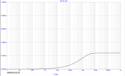
If Vcc = 63V, RL = 8 Ohms, Vout = 50Vpk, THD20 = 14ppm. BUT ... I think this figure is a bit pessimistic due to bad models of the MOSFETs. See the jagged residual (4th pic), which is highly unnatural. This is the result of discontinuities in the derivatives of the mathematical model.
As promised Vgs comes up tomorrow. I found a testing procedure on the net. Hope it works
Cheers,
Olivier
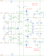
Below a new version using the current PCB plus a preliminary OPS. This one is equipped with separate push-pull drivers for the top- respectively bottom-MOSFETs (yes indeed, that's my favorite configuration
") ). But we have a problem in case of very low threshold fets (i.e. laterals), as the minimum differential OP voltage (between G1 and G2) of this kind of setup is >= 2*Vbe. That's too much for the laterals. By 'overlapping' the drivers 'voltage-wise' (sorry for my Dunglish) I was able to reduce aforementioned voltage to a range of 250 .... 1500mV. (notice C23 and Q29, they are placed 'upside down')
). But we have a problem in case of very low threshold fets (i.e. laterals), as the minimum differential OP voltage (between G1 and G2) of this kind of setup is >= 2*Vbe. That's too much for the laterals. By 'overlapping' the drivers 'voltage-wise' (sorry for my Dunglish) I was able to reduce aforementioned voltage to a range of 250 .... 1500mV. (notice C23 and Q29, they are placed 'upside down')BTW, this configuration can easily be modified to fit higher threshold fets, by means a few jumper. More on this later.
One point of caution: Don't torture the drivers with an unfiltered square wave, as peak currents will destroy them (most likely). In order to safely test the amp, you will need a second order LP filter at the input.
Probably you will have a lot of questions about this design, as it is a bit unusable. But first, let's get the Miller sim working.
See you tomorrow.
E.
Attachments
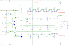
Vertical MOSFET driver
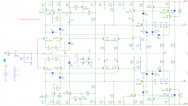
And here is the driver for higher threshold fets (2SK1530/2SJ201).
Also included a THD20 plot + residual. This one is much smoother, because the weak inversion (sub-threshold) is also modeled (BSIM3.3)
Driver components that has been changed (value and/or position):
C23, R44, R45, Q29, Q30, Q31 & D21. All you need for the PCB mod are two jumpers and eight extra holes.
Cheers,
E
Attachments
Hi Edmond,
Before I read your latest postings.
Here are te results for the 2SK1058 Vgs testing (just on 1 device) :
0,4V -> 35mA
0,7V -> 70mA
0,8V -> 100mA
0,9V -> 130mA
0,946V -> 150mA
1V -> 172mA
1,5V -> 400mA
I connected 10V to the drain through a 10E resistor and through a ampère meter.
I used the 2nd PSU channel to set the Vgs voltage. I read the voltage of Vgs on a voltmeter parallel over the 2nd PSU. I think it is right to do it that way.
Now I still don't know what the Vt is since the current ramps down but there is no real abrupt 'fall to zero' value ... but you asked especially for Vgs @ 150mA. I gues MC does the rest to draw the curve?
OK Now I will go for my 2SJ162 device ...
Cheers
Olivier
And here is the testresult for the 2SJ162
0,0V -> 7,4mA
0,3V -> 53mA
0,46V -> 90mA
0,68V -> 150mA
1,05V -> 261mA
1,59 -> 445mA
Then it ran a bit hot
By the way I did not mention in the 2SK1058 post (because I didn't expect the 2SJ162 to run current with no Vgs applied) that the 2SK1058 does not conduct at Vgs=0 (it is completely off).
I gues this means Vt is really low for both channels P & N.
I hope these results are useful for you ...
Now I go read your latest postings...
Cheers
Olivier
Edmond,
Just another question.
While measuring the output of the amplifier with input connected to generator but no signal applied. What is the highest Vpp of output rubble one can tolerate?
Right now I still have 2mV on the output of my OPS. There is a 50Hz component and also really noise. Is this good? Bad?
Maybe interesting to say : actually there is no input filtering at all.
Another strange thing I noticed while testing. On a 100KHz squarewave the rising and falling slope are visually identical. However the top slope nicely curves towards a flat line at 200V/us. On the down side idem but there seems to be a tiny little overshoot. But it does not look like ringing (no no) I will take a picture tomorrow.
Cheers
Olivier
Laterals
Hi Olivier,
Thanks for measuring the fets. I will incorporate your figures into the models.
As for the noise and hum, please let me think about it.
As for the tiny little overshoot, please, accept we don't live in a perfect world.
BTW, testing with a 100KHz square wave is an extreme torture (kind of waterboarding). Not every OPS will survive this.
Cheers,
E.
noise
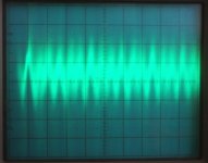
Hi Olivier,
The noise level also depends on the bandwidth (of course). Below you see a sim of the output noise as function of BW. Up to 1MHz the noise is 167uV RMS. The peak to peak value is of course much higher, at least three times, depending on the crest value.
Also have a look at the output of one of my own amps. The noise is mainly dominated by HF ingress (Y=2mV/div, X=0.5us/div, BW=1MHz).
Hope this helps.
Cheers,
E.
Edmond,
Just another question.
While measuring the output of the amplifier with input connected to generator but no signal applied. What is the highest Vpp of output rubble one can tolerate?
Right now I still have 2mV on the output of my OPS. There is a 50Hz component and also really noise. Is this good? Bad?
..........
Cheers
Olivier
Hi Olivier,
The noise level also depends on the bandwidth (of course). Below you see a sim of the output noise as function of BW. Up to 1MHz the noise is 167uV RMS. The peak to peak value is of course much higher, at least three times, depending on the crest value.
Also have a look at the output of one of my own amps. The noise is mainly dominated by HF ingress (Y=2mV/div, X=0.5us/div, BW=1MHz).
Hope this helps.
Cheers,
E.
Attachments
Pictures
Hi Edmond,
I am still not through your last postings about the OPS.
One thing on your schematic for the Front End : you changed the value of R16 & R17 to 100 Ohms. On the PCB actually they are bridged 0 ohms. I did that because I had oscillations on that node (both). However they were 1K resistors. Is 100E the best inbetween? How can this resistor cause oscillations anyway? It's a base resistor for the regulator Q, nothing more.
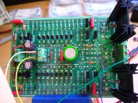
Hereby some pictures of the actual situation.
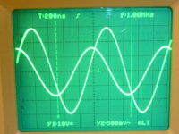
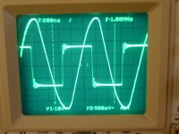
First the PCB itself. You can use it to see what components are in place, not placed and what components are placed on the fly (temporary placemnt). You see the simple millercaps flying there, bridging from R43 to R36 and R44 to R37. You can also see the different ground nodes (Signal Ground (the one on the full left upper screw), the feedback ground (top screw, middle terminalblock), the commonground (CGND see silkscreen), Decoupling Ground (middle screw, right terminalblock, green wire). As you notice very few capacitors are installed : only input DC blocking caps (C2A & C2B), 1 pair of decoupling caps C3 & C4 (the larger decoupling electrolyts are not installed C11 & C10), The lead-lag caps C12/13, the CMCL caps C15/16, and finally C8 the small cap across the Feedback cap C7 which is also installed). Not installed are : The right hand side decoupling caps (electrolyt C26/27 + polyprops C24/25) as stated before the left hand side decoupling electrolyt caps C10/11, the bias filter cap CB, the cascode zener voltage ref filter caps C22/23, the TMC caps C18->21), C17A&B (added at the last moment they are for stability but don't know how yet), C5/6 the stability caps at the right leg of the diff amps. Also C9/R19 feedforward is not installed. Also different protection components are not installed (diodes, resistors). The only protection installed are the VAS current limiter Q's.
Long story but hopefully means something to you.
Other pictures are :
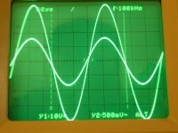
100KHz sine response
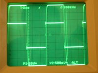
100KHz square response (the bottom overshoot is difficult to see but OK I read that is acceptable)
1MHz sine response
1MHz square response
You can see it is very near the ULGF -3dB point of the amplifier.
You can also see the square wave output is higher at 1MHz than the sine wave at 1MHz (why is that? output transitor input capacitance? diff amp capacitance?)
Also notice signal generator has some ringing on the square wave. Amp coops well with that I seem to believe. But is the generator supposed to do that? Bad generator or input of amplifier does this ?
One more thing about your OPS. Do you think Error Correction is on the order for this amplifier? (I hope it is not incorporated in your OPS yet as I would deserve a slap in the face ).
Cheers
Olivier
Hi Edmond,
I am still not through your last postings about the OPS.
One thing on your schematic for the Front End : you changed the value of R16 & R17 to 100 Ohms. On the PCB actually they are bridged 0 ohms. I did that because I had oscillations on that node (both). However they were 1K resistors. Is 100E the best inbetween? How can this resistor cause oscillations anyway? It's a base resistor for the regulator Q, nothing more.
Hereby some pictures of the actual situation.
First the PCB itself. You can use it to see what components are in place, not placed and what components are placed on the fly (temporary placemnt). You see the simple millercaps flying there, bridging from R43 to R36 and R44 to R37. You can also see the different ground nodes (Signal Ground (the one on the full left upper screw), the feedback ground (top screw, middle terminalblock), the commonground (CGND see silkscreen), Decoupling Ground (middle screw, right terminalblock, green wire). As you notice very few capacitors are installed : only input DC blocking caps (C2A & C2B), 1 pair of decoupling caps C3 & C4 (the larger decoupling electrolyts are not installed C11 & C10), The lead-lag caps C12/13, the CMCL caps C15/16, and finally C8 the small cap across the Feedback cap C7 which is also installed). Not installed are : The right hand side decoupling caps (electrolyt C26/27 + polyprops C24/25) as stated before the left hand side decoupling electrolyt caps C10/11, the bias filter cap CB, the cascode zener voltage ref filter caps C22/23, the TMC caps C18->21), C17A&B (added at the last moment they are for stability but don't know how yet), C5/6 the stability caps at the right leg of the diff amps. Also C9/R19 feedforward is not installed. Also different protection components are not installed (diodes, resistors). The only protection installed are the VAS current limiter Q's.
Long story but hopefully means something to you.
Other pictures are :
100KHz sine response
100KHz square response (the bottom overshoot is difficult to see but OK I read that is acceptable)
1MHz sine response
1MHz square response
You can see it is very near the ULGF -3dB point of the amplifier.
You can also see the square wave output is higher at 1MHz than the sine wave at 1MHz (why is that? output transitor input capacitance? diff amp capacitance?)
Also notice signal generator has some ringing on the square wave. Amp coops well with that I seem to believe. But is the generator supposed to do that? Bad generator or input of amplifier does this ?
One more thing about your OPS. Do you think Error Correction is on the order for this amplifier? (I hope it is not incorporated in your OPS yet as I would deserve a slap in the face ).
Cheers
Olivier
Attachments
- Status
- This old topic is closed. If you want to reopen this topic, contact a moderator using the "Report Post" button.
- Home
- Amplifiers
- Solid State
- HEEEELLLPPP : M. Randy Slone Mirror Image Topology Construction - Troubles