Hi Wahab,
> Using more cycles in sims didn't change the picture.
Hmm....
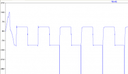
In my sim it took some time before the DC level got stable, see pic.
If the DC component is still drifting, I get a totally erroneous THD figure. If taken from the 1st cycle for example, THD20k = 18%, instead of 425ppm when taken from a stable cycle.
Apparently, you have tackled this problem in a different way.
Cheers,
E.
hI, Edmond
I clarify somewhat my tries, since one thing
was not correct..
When tested unloaded, the VAS+OPS open loop
configuration display more THD than the single VAS open loop.
With TMC implemented, the VAS + OPS show lower THD than
the single VAS open loop , thus , TMC reduce distorsion
of both stages..
But if the VAS + OPS is loaded , although implementing TMC
reduce significatly THD , it s still higher than with the single VAS,
this because the OPS produce high distorsion when loaded,
as the avalaible gain being less, there s no more enough NFB
to bring the said THD below the one of the single VAS.
THD increase by some 20db with a load, so the remaining
10db of NFB can in no way bring back THD to a lower or
even equal value than the single VAS one...
As for computing THD without influence of the DC
settling time, you must specify to your simulator that
the probe is AC coupled only.
Another solution is to insert a CR circuit is serial with the probe,
a cap of about 10mF in serial with the output and a 100 Megaohm
resistor from the cap probe side to ground , for computation
convergence purpose..
Hope that we will also both converge to a real solution..
")
cheers,
w
Last edited:
Various THD measurements
Hello Edmond
The following are THD measurents with circuit modifications at @20kHz 82Vpp (28Vrms) into 8 ohms (103Watts)
Amp without clamp THD 0.000276% 2.76ppm
Amp with clamp THD 0.000281% 2.81ppm
Amp with Boot strapped Clamp THD 0.000279% 2.79ppm
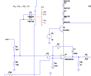
As can be seen the bootstrapped clamp gives the better performance than the non boot strapped clamp. But interestingly diodes D1 and D2 have to be individually boot strapped for the clamp to work in my hands I could not get your approach to work as tying the other ends of the diiode together created a problem . Attached is the schematic .
Regards
Arthur
Hello Edmond
The following are THD measurents with circuit modifications at @20kHz 82Vpp (28Vrms) into 8 ohms (103Watts)
Amp without clamp THD 0.000276% 2.76ppm
Amp with clamp THD 0.000281% 2.81ppm
Amp with Boot strapped Clamp THD 0.000279% 2.79ppm
As can be seen the bootstrapped clamp gives the better performance than the non boot strapped clamp. But interestingly diodes D1 and D2 have to be individually boot strapped for the clamp to work in my hands I could not get your approach to work as tying the other ends of the diiode together created a problem . Attached is the schematic .
Regards
Arthur
Attachments
Last edited:
Hi Arthur,Hello Edmond
[snip]
But interestingly diodes D1 and D2 have to be individually boot strapped for the clamp to work in my hands I could not get your approach to work as tying the other ends of the diode together created a problem.
Regards
Arthur
Hmm... That's a bit weird and against all logic. Perhaps it has something to do with a DC offset. Have a look at the voltages across the diodes (should be as small as possible). Maybe this will give a clue.
Cheers,
E.
Hi Arthur,
Hmm... That's a bit weird and against all logic. Perhaps it has something to do with a DC offset. Have a look at the voltages across the diodes (should be as small as possible). Maybe this will give a clue.
Cheers,
E.
Hello Edmond
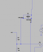
The voltage across is shown in the attachments, are these voltage low enough.
Regards
Arthur
Attachments
Bootstrapped clamp
Hello Edmond
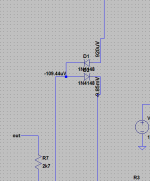
Here is the single boot strapped clamp.
ON Mosfets these guys will have 2SK1530 in late October, but they dont know what selection they will get until they get them in there hands they currently have the 2SJ201-Y. I buy stuff from them . If you would like a contact I can send you a private email.
Ten Four LTD
Regards
Arthur
Hello Edmond
Here is the single boot strapped clamp.
ON Mosfets these guys will have 2SK1530 in late October, but they dont know what selection they will get until they get them in there hands they currently have the 2SJ201-Y. I buy stuff from them . If you would like a contact I can send you a private email.
Ten Four LTD
Regards
Arthur
Attachments
hI, Edmond
I clarify somewhat my tries, since one thing was not correct..
When tested unloaded, the VAS+OPS open loop configuration display more THD than the single VAS open loop.
Hi Wahab,
OK. This can be explained by the (nonlinear) loading effect of the drivers.
With TMC implemented, the VAS + OPS show lower THD than the single VAS open loop, thus, TMC reduce distortion of both stages..
OK. But.....
1. By how much? 1dB or 10...20dB?
2. Due to what? The unloading effect or increased loop gain?
OKBut if the VAS + OPS is loaded , although implementing TMC reduce significantly THD, it s still higher than with the single VAS, this because the OPS produce high distortion when loaded, as the available gain being less, there's no more enough NFB to bring the said THD below the one of the single VAS.
THD increase by some 20db with a load, so the remaining
10db of NFB can in no way bring back THD to a lower or
even equal value than the single VAS one...
Agreed.
As for computing THD without influence of the DC settling time, you must specify to your simulator that the probe is AC coupled only. Another solution is to insert a CR circuit is serial with the probe, a cap of about 10mF in serial with the output and a 100 Megaohm resistor from the cap probe side to ground , for computation convergence purpose..
Hope that we will also both converge to a real solution..
cheers,
w
With MicroCap I can specify to ignore the DC component but it can't ignore the effect of DC drift.
Therefore, may I suggest to use another test circuit, that doesn't suffer from DC drift altogether?
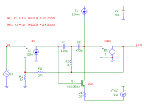
What about this one as shown below? An idealized 'blameless' amp, except the VAS, which is a 'real' tranny. The IPS is a transconductance stage with a gain of 20mA/V and the OPS is a simple voltage follower with a gain of 1. THD20k-TPC = 32.7ppm; THD20k-TMC = 29.5ppm.
Since the effect of TPC vs TMC is only marginal, I think that the slight improvement should only be attributed to the unloading of the VAS. If the VAS has benefited from TMC to the same extent as the OPS, then the improvement should be much higher, in the order of 10...20dB, which is not the case.
Cheers,
E.
Attachments
Hello Edmond
Here is the AC performance with the diodes tied together, with 1.5 V sine wave at input the output should be a sine wave.
Regards
Arthur
Hi Arthur,
Do I understand correctly that if you also connect the diodes together at the right side, the voltage across them rises from a few mV to several Volts???, that is, under normal operating condition. Why? Do I overlook something?
Cheers,
E.
MC9 circuit coversion
Hello Edmond
Attached is the circuit in MC9 format with the same models. All the circuit variations work in MC9 unlike what happens in LTSPICE although I get (check numeric output window for warnings) in MC9.
I am a little confused.
Please forgive my circuits for not being as neat and well drafted as yours.
Can this circuit be modified to accomodate ETMC and CMCL
Regards
Arthur
Attachments
Last edited:
Stupid error
I made a stupid error/typo. In the above text, TPC should read as conventional Miller compensation (CMC). So:
THD20k-CMC = 32.7ppm; THD20k-TMC = 29.5ppm.
Since the effect of CMC vs TMC is only marginal, I think that the slight improvement should only be attributed to the unloading of the VAS.
My humble apologies for the confusion.
Cheers,
E.
................
THD20k-TPC = 32.7ppm; THD20k-TMC = 29.5ppm.
Since the effect of TPC vs TMC is only marginal, I think that the slight improvement should only be attributed to the unloading of the VAS.
.....................
I made a stupid error/typo. In the above text, TPC should read as conventional Miller compensation (CMC). So:
THD20k-CMC = 32.7ppm; THD20k-TMC = 29.5ppm.
Since the effect of CMC vs TMC is only marginal, I think that the slight improvement should only be attributed to the unloading of the VAS.
My humble apologies for the confusion.
Cheers,
E.
Jooh !
Hi everyone,
Here is version 11 of the amp I would like to construct.
It is based on Slones Mirror Image Topology with Current Mirrors but compensated with a CMCL as presented by Edmond.
Edmond,
It contains your earlier version of VAS Clamp. Is this implemented correctly?
It uses your earlier version of CMCL I believe the one in your RS1 circuit.
I feel more comfortable with that one. Is it realy quite more noisy than the later versions in RS3 & RS4?
I lowered the Iq's through the KSA1381 and counterpart a lot to stay at maximum 6mA in the VAS legs and 7mA in the OPS driver legs. I believe this is well within the SOAR but they will need some Heatsinking, I know.
I did it because it is a 300V component and intending for 80 to 85V railvoltage, some other usual components are 160V or 180V limited which is close when we sum both rail voltage.
I really think the OPS drivers at 7mA will never go out of class A because MOSFETS draw very low gate currents and do not suffer Beta Droop.
You once mentioned a high peak current. But in my simulation it is still low enough even in full square wave. And hey, as you said, why bother if we slip slightly into class AB while blowing up our tweeters sending them 300W vertikal ramp voltages !?!
My only bothering is that the OPS itself has devices specified for 160V only. In class B as they are it shouldn't be a big concern I thought but you said it is different. Why? In case of shortcircuit failure of one, it is true 2Vrail will stand accros the other one if there is no speaker. But I guess this triggers the protection or fuse fast enough since these Mosfets are really forgiving. Could you shed some light here?
The Slew Rate : around 60V/uS
THD 300W 8ohm 20Khz --> 10ppm at 200KHz // 5ppm at 100KHz
THD 300W 8ohm 1Khz --> 0,4ppm at 200KHz // 0,4ppm at 100KHz // 0,1ppm until 48KHz.
What bothers me most is the AC analyses. In this world it is OK but in the real world the PCB , shielding etc will have to be too perfect to avoid instability or generating higher frequencies sitting on the real signal.
For the internal Response (that is between Vout before ZOBEL and at the inverting input that is after the input conditioning circuit).
-3dB point @ 1MHz (!!!! OMG !!!!)
It goes through 0dB at near 22MHzeek:)  ?
?
What do you think of the proctecion circuit? For now it is SLONES multislope (commercial variant for higher power amps).
It also still contains the Cascode stage. Tomorrow I will see what the distortion does when I remove it.
Good Night
Olivier

Hi everyone,
Here is version 11 of the amp I would like to construct.
It is based on Slones Mirror Image Topology with Current Mirrors but compensated with a CMCL as presented by Edmond.
Edmond,
It contains your earlier version of VAS Clamp. Is this implemented correctly?
It uses your earlier version of CMCL I believe the one in your RS1 circuit.
I feel more comfortable with that one. Is it realy quite more noisy than the later versions in RS3 & RS4?
I lowered the Iq's through the KSA1381 and counterpart a lot to stay at maximum 6mA in the VAS legs and 7mA in the OPS driver legs. I believe this is well within the SOAR but they will need some Heatsinking, I know.
I did it because it is a 300V component and intending for 80 to 85V railvoltage, some other usual components are 160V or 180V limited which is close when we sum both rail voltage.
I really think the OPS drivers at 7mA will never go out of class A because MOSFETS draw very low gate currents and do not suffer Beta Droop.
You once mentioned a high peak current. But in my simulation it is still low enough even in full square wave. And hey, as you said, why bother if we slip slightly into class AB while blowing up our tweeters sending them 300W vertikal ramp voltages !?!
My only bothering is that the OPS itself has devices specified for 160V only. In class B as they are it shouldn't be a big concern I thought but you said it is different. Why? In case of shortcircuit failure of one, it is true 2Vrail will stand accros the other one if there is no speaker. But I guess this triggers the protection or fuse fast enough since these Mosfets are really forgiving. Could you shed some light here?
The Slew Rate : around 60V/uS
THD 300W 8ohm 20Khz --> 10ppm at 200KHz // 5ppm at 100KHz
THD 300W 8ohm 1Khz --> 0,4ppm at 200KHz // 0,4ppm at 100KHz // 0,1ppm until 48KHz.
What bothers me most is the AC analyses. In this world it is OK but in the real world the PCB , shielding etc will have to be too perfect to avoid instability or generating higher frequencies sitting on the real signal.
For the internal Response (that is between Vout before ZOBEL and at the inverting input that is after the input conditioning circuit).
-3dB point @ 1MHz (!!!! OMG !!!!)
It goes through 0dB at near 22MHz
eek:) ?What do you think of the proctecion circuit? For now it is SLONES multislope (commercial variant for higher power amps).
It also still contains the Cascode stage. Tomorrow I will see what the distortion does when I remove it.
Good Night
Olivier
Attachments
I cannot test without Cascode here (on the job) but something crossed my mind on another point.
I already tried to lower the AC performance of this amp.
I would like it to have its -3dB point at around 100-300KHz and I would like it to go down the 0dB point at around 1MHz or a bit more depending on the first, since I guess it's -20dB/Decade anyway, starting from 34dB I will need 1,5 decade.
Adapting the input circuit ?
-> this is not going to resolve the internal figures of the AC analyses right?
OK it will prevent from RF to come into the input but it could still be pickedup inside the amp...
Raising the miller caps ?
-> This raises the distortion dramatically at high freq. it goes easily from 10ppm to 50ppm and higher when increasing lets say from 75pF to 82pF or 100pF ... And it doesn't even reduce my AC plot a lot
-> It also slows the amp, reducing slewrate...
Raising other internal caps?
-> this is somewhat out of my league but I suppose it can reduce innstability by narrowing the bandwidth at some places. Like Edmond added small 39pF caps at the current mirror bases, adding caps from the link between IS and VAS to the rail.
Is this the best solution?
Or comes it simply down to the fact that :
You like low THD? You are going to have to live with its troubles of taming its AC response by designing top notch pcb's (with ground layers, shieldings, twistings, choosing carefully the T points, etc...) and when it oscillates -> try to locate the origin and implement countermeasures at this particular point.
Until later ... byebye
Olivier
Hello Edmond
Attached is the circuit in MC9 format with the same models. All the circuit variations work in MC9 unlike what happens in LTSPICE although I get (check numeric output window for warnings) in MC9.
I am a little confused.
Please forgive my circuits for not being as neat and well drafted as yours.
Can this circuit be modified to accommodate ETMC and CMCL
Regards
Arthur
Hi Arthur,
I've simmed your circuit too and it works as expected.
As I don't have a 100 inch flat screen, I've shrunken your schematic a little bit
and remedied the warnings (see phoenix1).In version-2 I've lowered the ULGF of the second Miller loop (C2 & C3) to a safer level: from 3Mhz to 1 MHz (by adjusting R9 & R10) and increased the OPS bias to compensate for higher distortion. Also, I've added a kind of 'bleeder resistors' R7 & R8. Together with D1 & D2 plus bootstrap, these guarantees that no current leaks to the inverting input (under normal conditions, of course). At high output voltages (50V) at least one of these two measures are necessary, but to be on the safe side, I would do both.
>Can this circuit be modified to accommodate ETMC and CMCL
In principle, yes. But it's not that easy. If you don't mind, I'm not going to figure out how exactly, as I'm not specialized in BJT output stages and already a few month behind schedule. Sorry.
Cheers,
E.
Attachments
Stuff
Hello Edmond
Thanks for the reworking and I appreciate your effort and time. I would like to ask you a few question on Pheonix 2 . The C4( 8pf) how did you came to this value. How do you check the phase margin of the clamp .
The attached file shows an attempt at how you measure phase margin and ULG is this how you do it. On other R15 and R16 should be 22R its best in practice and in simulation.
I gave a link a couple of threads back for TEN FOUR LTD , did you pick it up they can get the Mosfets that your are after. Have you sorted the supply of these parts.
Regards
Arthur
Attachments
Hello Edmond
Thanks for the reworking and I appreciate your effort and time. I would like to ask you a few question on Pheonix 2 . The C4( 8pf) how did you came to this value.
Hi Arthur,
I did it the empirical way. Just run an AC or trans. sim and select C4 for the lowest voltage across the clamping diodes at say 20...100kHz. (see my *.CIR files)
How do you check the phase margin of the clamp.
I didn't check it yet. A simple way it to apply a DC voltage of 2...3V at the input and put a gain probe between the diodes and the inverting input of the op-amp.
The attached file shows an attempt at how you measure phase margin and ULG is this how you do it.
This is how you get the open loop response. Feedback loops have to be determined in another way. There are two of them: an inner loop and an outer (or global) FB loop. See the attached files and run the AC analysis.
In the mean time I've changed the Miller compensation a little bit: I've moved the take off point to the emitters of the pre-drivers (instead of the VAS output). The reason why I've done this is because the VASes themselves have no current gain (just 1x), so hardly any Miller effect. Including the pre-driver inside the Miller loop provides the necessary gain.
Next, we have to choose appropriate values for the FB resistors to the op-amp output. R11, C2 and C3 determine the ULGF of the inner loop: 1/(2*pi*R11*(C2+C3))
Appropriate values lie between 0.5 and 2MHz. For 1MHz, and C2=C3=47pF, R10 becomes 1k5. Next, we have to choose a suitable ratio between R11 and R10. It should be considerably lower than the closed loop gain (CLG=R3:R4), but not to low, otherwise the op-amp can't handle the voltage swing. As a rule of thumb I set it to about sqrt(CLG), so R10 ~= 270 Ohms. In this case the max. output voltage of the op-amp is 8V.
Run an AC analysis on PHEONIX3-Inner-Loop.CIR to verify the ULGF and phase margin (PM)
Now we have to choose appropriate values for R9 and C2 in such a way that not only the ULGF of the outer loop is the same as the inner loop, but also the (closed loop) step response is critically damped.
This is not as strait forward as in the previous case, as several factors are involved. I think the fastest method is an iterative process and/or a little bit of trial and error. We first start by setting C2 = (C3+C4) * (R11/R3) * (R10+R11)/R10 = 408pF -> 390pF and set R9=0
If you run PHEONIX3-Outer-Loop.CIR you will get an ULGF of 800kHz. Almost good, but at 1MHz the phase response deviates from 90 deg. by as much as 20 deg. and I don't like that. With R9 = 220R, the response is much nicer: ULGF = 980kHz and PM = 87 deg, almost perfect. Now check the step response. In this case it was okay, though in many other cases I had to adjust the components for a better step response, then check the ULGF and PM again, etc. etc.
On other R15 and R16 should be 22R its best in practice and in simulation.
In what respect? better stability, lower THD? According to John Curl (and many others) 4.7R is optimal
I gave a link a couple of threads back for TEN FOUR LTD, did you pick it up they can get the Mosfets that your are after. Have you sorted the supply of these parts.
Regards
Arthur
I'm almost out of supply, so I visit that website, but got the message: "No matching part numbers found". So, what next?
BTW1, distortion is slightly higher compared to your previous design, but I think better stability is preferable over lower THD at the expense of the phase margin.
BTW2, as you see, now the resistors at the output of the op-amp are much higher, instead of those stupid hot running R's like in the Alexander amp.
BTW3, we are still not done!!! PM check of the compensating and clamp loops, output stage protection, HF input filter, bias generator, Zobel thingy, SOA checks, 15V regulators, etc.
Cheers,
E.
Attachments
Last edited:
- Status
- This old topic is closed. If you want to reopen this topic, contact a moderator using the "Report Post" button.
- Home
- Amplifiers
- Solid State
- HEEEELLLPPP : M. Randy Slone Mirror Image Topology Construction - Troubles