Very nice buildIt was something that I appreciate, thanks for sharing information anyway.
I already build a P3A amplifier.
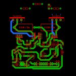
Here is the pictures View attachment 1073728 View attachment 1073729 View attachment 1073730
I just love to build new project and then move on to new project, it's fun doing this audio amplifier stuff, I do it only for fun.
No commercial activity.
I like it.
I notice VIPINSAINI20, in your attached image above, that you have used FR4 laminate as a substitute for sheet metal to thermally couple driver transistors with the Vbe multiplier transistor. This may work in a steady state but have a very slow response to audio signal level variations and limits the potential of the design. The epoxy/glass material will dramatically damp and slow the heat transfer of the very thin copper foil and consequently, actual bias will probably have little relationship to optimum.
Simply use a piece of approx. minimum 1mm sheet aluminium or copper. Alternatively, just strap Q9 directly to Q5 or Q6, as the ESP image and other recent builds will illustrate.
Simply use a piece of approx. minimum 1mm sheet aluminium or copper. Alternatively, just strap Q9 directly to Q5 or Q6, as the ESP image and other recent builds will illustrate.
Last edited:
I understand your point about thermal tracking.I notice VIPINSAINI20, in your attached image above, that you have used FR4 laminate as a substitute for sheet metal to thermally couple driver transistors with the Vbe multiplier transistor. This may work in a steady state but have a very slow response to audio signal level variations and limits the potential of the design. The epoxy/glass material will dramatically damp and slow the heat transfer of the very thin copper foil and consequently, actual bias will probably have little relationship to optimum.
Simply use a piece of approx. minimum 1mm sheet aluminium or copper. Alternatively, just strap Q9 directly to Q5 or Q6, as the ESP image and other recent builds will illustrate.
And it's not glass epoxy material, but it's is a fr4 dual sided copper clad indeed.
Anyway
I did that because I just wanted to play with p3a amplifier for fun, I didn't build that amplifier for long term use, I just build them, power up them, play some sounds on them, do a power test and then, amplifier just kindly sits on my bin or desk collecting dust,
And I move on to new play thing
If I happened to make a long term plan to use such amplifier, I will surely remember your suggestion
Thanks anyway.
Yes, I probably could have fully described the copper foil layers as well, though it is usually assumed unless noted, to mean a standard grade with 30-35μm copper foil thickness.
Just for the record (from Wikipedia): FR-4 (or FR4) is a NEMA grade designation for glass-reinforced epoxy laminate material. FR-4 is a composite material composed of woven fiberglass cloth with an epoxy resin binder that is flame resistant (self-extinguishing).
Good luck with the next build too - it's great to see what projects and details interest people and to understand their reasons.
Last edited:
Do you have any other design layout available for 60W~100W amplifier.Simply use a piece of approx. minimum 1mm sheet aluminium or copper. Alternatively, just strap Q9 directly to Q5 or Q6, as the ESP image and other recent builds will illustrate.
I plan to build a new 6 channel amplifier using such circuit. But I don't have small and compact layout for p3a, otherwise p3a is very good amplifier,
Alex MM design p3a layout is small and compact enough for me but sadly he didn't share the pdf files for his p3a project.
Here is a picture of Alex MM p3a layout
I need something similar to this compact version ,it's very good 74x58 mm.
If you know Someone who have this layout please share black and white toner transfer working files.
Although I seen FH9 FH11 and etched some pcbs for testing but I haven't Assembled them, due to lack of interest, I don't have many IRFP240 IRFP9240 mosfet in stocks only 6 pair left, but I do have bjt like
1. NJW0281G NJW0302G 34 Pairs
2. 2SC5200 2SA1943 13 Pairs
3. C5200N 20pcs
4.C5198 A1941 50 Pairs
5. C4382 A1668 17pairs
6. C5171 A1930 10pair
7. C4793 A1837 40pairs
8. Other TO-92 transistors
2N5551, 2N5401 Fairchild , BC546B Fairchild, BC556 Philips
And I don't want to buy new mosfet devices,
So ,
I have a kind Request
Please share something solid, which I can use in my amplifier for long term.
I have heatsinks with dimensions 303x32x99mm 2pcs each 1.3KG
Transformer 800VA
36-0Vac, 2.4A 6 windings
40-0Vac ,2.4A 2 winding
I plan to build a capacitance multiplier and psu, so DC voltages should be somewhere between 42-0-42VDC 5~6 volts may lost between Diodes and Capacitance multiplier and PSU
So recommend something with maximum 50-0-50 vdc power supply.
Here is my email address vks.vper.rpvv@gmail.com and WhatsApp number 8920599797
I like your information about this.Yes, I probably could have fully described the copper foil layers as well, though it is usually assumed unless noted, to be a standard grade with 30-35μm copper foil thickness.
Just for the record (from Wikipedia): FR-4 (or FR4) is a NEMA grade designation for glass-reinforced epoxy laminate material. FR-4 is a composite material composed of woven fiberglass cloth with an epoxy resin binder that is flame resistant (self-extinguishing).
But the Dual layer copper clad I used isn't made of fiberglass, it's flame resistant, but isn't made of any kind of fibers.
I cut it, I drill into it and I also tried to burn it, it's made of some fine powdered material,
When I etched some pcbs, I try to look for fiberglass but I haven't find it yet, and it's softer than FR4 Glass Epoxy Copper Clad which I used in P3A pcbs, fiberglass copper clad is difficult to drill but the Dual layer copper clad I have is something else, which is softer to drill into.
And something interesting happened when I accidentally over heated the tracks, when I was Soldering the components.
If you overheat fr4 glass epoxy copper clad, the copper layer gets separated from epoxy material, and sometimes you can also see some separation between epoxy and fiberglass layers, and some bubble beneath and between copper layers and fiberglass and epoxy material itself.
But In case of the thing I have in Dual layer copper clad it doesn't happened it's just gets decoloration and some burning marks but no separation between clad materials, although if you overheat up right after etching the pcbs ,no time time drying process copper tracks may come off very quickly
Heh, heh. - If you cut, drill or grind the laminate, the glass fibre will soon shatter to dust and the only way to see the woven glass fabric would be to look at the cut edges and finely rippled surface under a strong light. You could also grab a strip of the stuff with pliers and twist it until the fabric splits apart and then see the fibrous patterns inside.
It's possible that you have a different (non-FR4) laminate material based on say, Polyvinyl alcohol, Kevlar or some other synthetic fabric that is compatible with epoxies, for example. Its unusual though, to find such materials outside special applications in industries supporting military, aerospace or other demanding applications.
Anyway, unless you have acquired some PCB laminate that isn't FR4 but perhaps based on synthetic fibre, it will really be glass fibre, just like like most PCBs now, globally and in many other products from roofing to boat hulls, light aircraft and electrical safety insulation. Its amusing too, that the older phenolic and urea resin boards that all the most popular Japanese audio products and reputations for high quality were built on, were reinforced with only Kraft paper!
I'll share the details about Dual layer copper clad later, when I find out the etched pics and some non etched ones in my bins, right now it's messy and stuff is everywhere, I'm arranging my stuff right now and checking how much and how many transistors and capacitors, I have around in my stocks, I'll share a video of copper clad, just drop your email or WhatsApp number or I have to upload it to Google drive or YouTube for better optionsHeh, heh. - If you cut, drill or grind the laminate, the glass fibre will soon shatter to dust and the only way to see the woven glass fabric would be to look at the cut edges and finely rippled surface under a strong light. You could also grab a strip of the stuff with pliers and twist it until the fabric splits apart and then see the fibrous patterns inside.
It's possible that you have a different (non-FR4) laminate material based on say, Polyvinyl alcohol, Kevlar or some other synthetic fabric that is compatible with epoxies, for example. Its unusual though, to find such materials outside special applications in industries supporting military, aerospace or other demanding applications.
Anyway, unless you have acquired some PCB laminate that isn't FR4 but perhaps based on synthetic fibre, it will really be glass fibre, just like like most PCBs now, globally and in many other products from roofing to boat hulls, light aircraft and electrical safety insulation. Its amusing too, that the older phenolic and urea resin boards that all the most popular Japanese audio products and reputations for high quality were built on, were reinforced with only Kraft paper!
Ask for someone who can delete components using corel draw or photoshop.Do you have any other design layout available for 60W~100W amplifier.
I plan to build a new 6 channel amplifier using such circuit. But I don't have small and compact layout for p3a, otherwise p3a is very good amplifier,
Alex MM design p3a layout is small and compact enough for me but sadly he didn't share the pdf files for his p3a project.
Here is a picture of Alex MM p3a layout
View attachment 1073887
I need something similar to this compact version ,it's very good 74x58 mm.
If you know Someone who have this layout please share black and white toner transfer working files.
Although I seen FH9 FH11 and etched some pcbs for testing but I haven't Assembled them, due to lack of interest, I don't have many IRFP240 IRFP9240 mosfet in stocks only 6 pair left, but I do have bjt like
1. NJW0281G NJW0302G 34 Pairs
2. 2SC5200 2SA1943 13 Pairs
3. C5200N 20pcs
4.C5198 A1941 50 Pairs
5. C4382 A1668 17pairs
6. C5171 A1930 10pair
7. C4793 A1837 40pairs
8. Other TO-92 transistors
2N5551, 2N5401 Fairchild , BC546B Fairchild, BC556 Philips
And I don't want to buy new mosfet devices,
So ,
I have a kind Request
Please share something solid, which I can use in my amplifier for long term.
I have heatsinks with dimensions 303x32x99mm 2pcs each 1.3KG
Transformer 800VA
36-0Vac, 2.4A 6 windings
40-0Vac ,2.4A 2 winding
I plan to build a capacitance multiplier and psu, so DC voltages should be somewhere between 42-0-42VDC 5~6 volts may lost between Diodes and Capacitance multiplier and PSU
So recommend something with maximum 50-0-50 vdc power supply.
Here is my email address vks.vper.rpvv@gmail.com and WhatsApp number 8920599797
")

I have test two versions of pcb for P3A.
The first version using Alexx mm pcb.
The second using the original pcb (previous ver.)
During test,i have sheen HUGE diference in IMD distortion!
Alex mm pcb was the undisputed winner.
Last edited:
Really isn't that cheating, looks like I have to be a greedy and selfish person now.Ask for someone who can delete components using corel draw or photoshop.
I don't have any one who can do it,
Looks like I have to visit cyber cafe for photoshop's work, and I don't have any idea about corel draw program, I never used it, because I don't have any computer in my house. 😑
But looks like this is the way to go if I want my amplifier to get ready
Okay
P
If you are getting trouble with PCB layout then you can easily build it on zero board or PCB. It just uses few componemts. I have built it and it works good.
dear friend p3a is not complicated amplifier.Really isn't that cheating, looks like I have to be a greedy and selfish person now.
I don't have any one who can do it,
Looks like I have to visit cyber cafe for photoshop's work, and I don't have any idea about corel draw program, I never used it, because I don't have any computer in my house. 😑
But looks like this is the way to go if I want my amplifier to get ready
Okay
If you are getting trouble with PCB layout then you can easily build it on zero board or PCB. It just uses few componemts. I have built it and it works good.
Did you get the files for Alex mm p3a by him or you did something similar corel draw or photoshop'sAsk for someone who can delete components using corel draw or photoshop.
I have test two versions of pcb for P3A.
The first version using Alexx mm pcb.
The second using the original pcb (previous ver.)
During test,i have sheen HUGE diference in IMD distortion!
Alex mm pcb was the undisputed winner.
If you did it already can't you be a little more kind to me, and share your layout with me.
I'm not a commercial actor here.
I do it only for fun and fun .
It's not the problem, if I have to build something on zero pcbs ,then I should get a little more time and draw a layout regardless if someone helps out or not, yeah my layout may contain errors or some routing problems but it's worth it.P
dear friend p3a is not complicated amplifier.
If you are getting trouble with PCB layout then you can easily build it on zero board or PCB. I have built it and it works good.
Don't worry about it, man I'll do something about it.
I just don't wanna be a copy paste person but it's the only way out of this problem,sadly, 😑
Ok I dear I understand your problem.It's not the problem, if I have to build something on zero pcbs ,then I should get a little more time and draw a layout regardless if someone helps out or not, yeah my layout may contain errors or some routing problems but it's worth it.
Don't worry about it, man I'll do something about it.
I just don't wanna be a copy paste person but it's the only way out of this problem,sadly, 😑
I could help you but problem is same I have never use PCB layout making softwares before on PC..
Don't worry about it, I'll manage some howOk I dear I understand your problem.
I could help you but problem is same I have never use PCB layout making softwares before on PC..
Than
Thanks for your kindness
Thanks for sharingI created alex mm pcb toner transfer image file sometime ago.
Check attachment. Size should be correct, check jpg image and mono file to compare. I didn't build yet due to other activities..
Thanks for your kindness
Good morning everyone. I'm making a different layout, based on Alexmm's layout. I have a question, do the tracks that leave the collector of Q5 and Q6 to the bases of the output TRs need to be the same size, according to the layout rules? Will different sizes detract from functionality? Grateful!
Attachments
Before improvising a new the design, you might want to enquire about the thermal stability of your layout.I'm making a different layout...
If you read the original info on ESP web site, you will learn that additional transistors are required to be in contact.
Cheers.
Why is it necessary to add transistors in the circuit? I think because of translation problems I didn't understand your comment.Before improvising a new the design, you might want to enquire about the thermal stability of your layout.
If you read the original info on ESP web site, you will learn that additional transistors are required to be in contact.
Cheers.
- Home
- Amplifiers
- Solid State
- P3A Comparison table ( long .... )