Hello everybody. Is anyone psb Apex AX14 with 2 pairs on the output?
Attachments
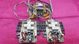


Where can i find Apex v14 with 2 pairs , schematic? Thank you!
Hope you're lucky.
A Directory of Apex Audio Amplifiers
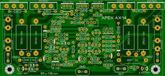
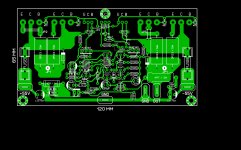
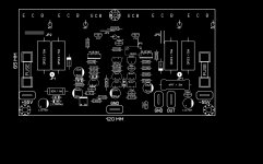
No. If you don't find it, it's not too difficult to work out. Quickly comparing it with the original schematic in post #1 :
- R21,22,23,24, Q12 and Q14 are doubled up, as you would expect.
- C13 has been replaced with 10R and 2 x 1N4148 all in parallel, ground loop breaker.
Also there must be link between points J-A and J-A1, not shown on the layout.
I'll leave it with you to follow through the rest of it for any other changes.
Looks like quite a nice single sided layout, I may use it myself, when I ever get round to it.
Simon
If anibody have any sugestions.. post please.
Attachments
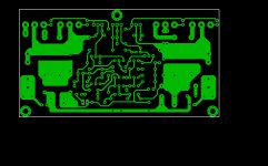
If anibody have any sugestions.. post please.
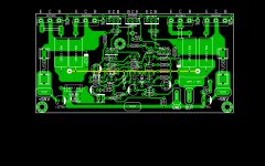
Any differences in this pcb design and one mentioned in post 10561
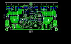
No. If you don't find it, it's not too difficult to work out. Quickly comparing it with the original schematic in post #1 :
- R21,22,23,24, Q12 and Q14 are doubled up, as you would expect.
- C13 has been replaced with 10R and 2 x 1N4148 all in parallel, ground loop breaker.
Also there must be link between points J-A and J-A1, not shown on the layout.
I'll leave it with you to follow through the rest of it for any other changes.
Looks like quite a nice single sided layout, I may use it myself, when I ever get round to it.
Simon
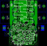
schematic in post #1 is not final. the one in post # 22 is, IMHO.
regards
Prasi
Circuit was tested on +/-90V rail voltage, but with single pair 2SC5200/2SA1943 +/-56V is maximum. 80W on 8R load with low THD.
Regards
Just wanted to check what an appropriate rail voltage would be for the AX14 with dual 2SC5200?
I have a choice of 35-0-35v and 47-0-47v trannies.
Can either be used without issue?
Cheers!
Hi Katiyar,
None of the items are from offline shops. Most of the items are from an Aliexpress seller who sells genuine parts . And some are from taydaelectronics.
Thank you
Sha
Can you share link of Ali Express dealer.
Thanks
- Home
- Amplifiers
- Solid State
- 100W Ultimate Fidelity Amplifier