Hello, don't be sorry friend... I appreciate every comments to improve the design of this layout.
Would you mind to state what would be the possible issue of the currently design to improve??
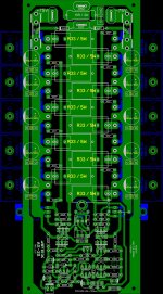
Pls. note SG is not directly connected to GND.
Thanks for the inputs...
What I was referring to is not related to the sig-ground, but to the main ground itself, which completely surrounds the whole board. I think it might be a good idea to break that big loop all around, so as to avoid making that loop.
Perhaps the break in that loop might be better if it's as far away from the main gnd connection, so somewhere at the opposit end of the board, where the input in located. Not sure which exact location is best and how big of a gap would be good, but it could be near the middle on the board end where the input is...
One other thing I would bring up, since this is a 5 pair output, it might also be a good idea to add a decoupling cap on each and every output transistor's collector. This part is quite easy to do, as there is plenty of room left there and they can be placed in a way that decouples the collector as close as possible to the transistors and jump to ground that is nearby. The changes to the layout would be minimal and this might be a good improvement for better stability.
Just my 2 cents...
It's me again.
I just thought of one more very tiny but perhaps useful adjustment.
Without actually changing the layout, the power transistor's emitter resistors could be some non inductive type, which some are in cases like TO220, TO126 or perhaps something similar. Those have a much smaller footprint but could fit in the same spot, more or less, as the existing power resistors. All that could be needed is extra holes/pads in a closer location to allow for either type of power resistor to be soldered in.
The non inductive resistors are rather expensive and not so easy to find, but some may want to use them. I would even use them myself, with a heatsink on them.
What I was referring to is not related to the sig-ground, but to the main ground itself, which completely surrounds the whole board. I think it might be a good idea to break that big loop all around, so as to avoid making that loop.
Perhaps the break in that loop might be better if it's as far away from the main gnd connection, so somewhere at the opposit end of the board, where the input in located. Not sure which exact location is best and how big of a gap would be good, but it could be near the middle on the board end where the input is...
One other thing I would bring up, since this is a 5 pair output, it might also be a good idea to add a decoupling cap on each and every output transistor's collector. This part is quite easy to do, as there is plenty of room left there and they can be placed in a way that decouples the collector as close as possible to the transistors and jump to ground that is nearby. The changes to the layout would be minimal and this might be a good improvement for better stability.
Just my 2 cents...
It's me again.
I just thought of one more very tiny but perhaps useful adjustment.
Without actually changing the layout, the power transistor's emitter resistors could be some non inductive type, which some are in cases like TO220, TO126 or perhaps something similar. Those have a much smaller footprint but could fit in the same spot, more or less, as the existing power resistors. All that could be needed is extra holes/pads in a closer location to allow for either type of power resistor to be soldered in.
The non inductive resistors are rather expensive and not so easy to find, but some may want to use them. I would even use them myself, with a heatsink on them.
Thanks... I noted the following points and will udjust the board accordingly, also I think 1,000uf/100v decoupling caps would be enough each power transistor(collector to ground)? Let me know your thoughts.
Thanks... I noted the following points and will udjust the board accordingly, also I think 1,000uf/100v decoupling caps would be enough each power transistor(collector to ground)? Let me know your thoughts.
Ouch!!! No, 1000uF is not what I had in mind for decoupling, I was only thinking about HF decoupling, perhaps with 100nF (x10 transistors).
But you could ponder adding a couple of 4700uF or something like that, right after the fuses, just for extra filtering on the power. Since there is a separate PSU board with plenty of filtering caps, that would be more than enough.
One thing that I'm not comfortable with, because you're aiming at +/-75V rails, I think the BC546 and also perhaps the BD139 would be too close for comfort on their Vceo. Using higher voltage ones might be a good idea.
Adding 10 decoupling caps doesn't add that much to the cost and layout, but their presence may help keeping it more stable I think.
Now that I think of it, I was also wondering about the negative end of C4 and also the common of R12/R13 that are going to sig-gnd. Wouldn't those be better on the main ground?
And if I get this right, the sig-gnd gets tied up to the main ground only via that C13 cap? is that correct??
Oppss sorry i misunderstood that... but adding 4700uF will be too big and will increase the size of the board, i think 100nf X10 each power transistor will be fine also in separate PSU with plenty of fitering caps will do the job.
Hi andrew,Local decoupling at the current consuming devices often does a lot of good and rarely causes problems.
The HF decoupling would be ~100nF at each device power pin.
The MF decoupling would be ~100uF to 470uF near each device power pin.
So is it a good idea a pair of 100nf and 100uf X10 near to each power device?
Last edited:
One HF and one MF decoupling cap from Power side to Power ground will probably be enough for each output device.
Gootee has suggested that multiple parallels will give better HF performance. I have no data to support either his or my recommendation.
I do believe that the HF decoupling grounds need to be connected together from the +ve side and the -ve side, to create the Power Ground.
Bringing the MF Decoupling and the Output Zobel/s to this same Power Ground seems to resolve all the above audio frequency signals that are floating around an audio amplifier.
It's this Power Ground that must be kept separate from the Signal Ground. Each of these Grounds require a link to the Main Audio Ground, whether it is on the PCB, or off board but nearby.
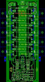
Willy what are the component numbers from the circuit diagram for the 22 uF and 100 nF on bottom of pcb.
Regards
Vostro i don't understand what you mean 22uf and 100nf on the bottom of the pcb, can you indicate on the pic?
Zobel network cap notification is mistake and now have change to 100nf.
Last edited:
Willy what are the component numbers from the circuit diagram for the 22 uF and 100 nF on bottom of pcb.
Regards
Sorry i think you're asking for C13 and C5.
Attachments
")
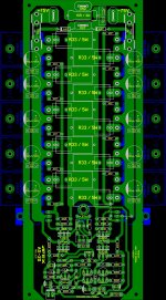
Nice concept idea Willie making the semiconductor blue to transfer the mounting of the transistor I like it
Regards
Juan
Thanks bro...
Regards,
Wil,
I said
You have two separate traces with an enormous loop. That introduces enormous inductance and completely ruins the ability of the HF decoupling to perform.
I said
You have not connected the + side to the - side.the HF decoupling grounds need to be connected together from the +ve side and the -ve side
You have two separate traces with an enormous loop. That introduces enormous inductance and completely ruins the ability of the HF decoupling to perform.
Wil,
I said
You have not connected the + side to the - side.
You have two separate traces with an enormous loop. That introduces enormous inductance and completely ruins the ability of the HF decoupling to perform.
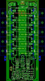
Opss sorry i miss this.. you mean like this??
Attachments
the ground trace of the +ve side must be the same ground trace for the -ve side.
Done this way the HF decoupling can connect from the device power pin to the common ground and then from that SAME common ground to the other polarity power pin.
You have two completely separate ground traces.
Done this way the HF decoupling can connect from the device power pin to the common ground and then from that SAME common ground to the other polarity power pin.
You have two completely separate ground traces.
the ground trace of the +ve side must be the same ground trace for the -ve side.
Done this way the HF decoupling can connect from the device power pin to the common ground and then from that SAME common ground to the other polarity power pin.
You have two completely separate ground traces.
Referring to the attached pic if you can see the ground trace from the top running both sides of + and - rails, is this considered as 2 different ground trace even they are connected in the same track from top to both +/-sides??
What's the preffered value for that cap that connect the +ve to -ve??
Attachments
Last edited:
I have not experimented with a Rail to Rail decoupling cap. In my mind that makes sense for a fully balanced power amplifier (and presumably for a balanced opamp) where there is NO GROUND CURRENT returning from the load.
The two separate ground traces have a long connection that is NOT ZERO IMPEDANCE.
The HF decoupling ONLY works when the returning Ground Currents can pass through what is effectively a near zero impedance. The +ve side HF cap and the -ve side HF cap MUST be connected together to achieve the NEAR ZERO IMPEDANCE.
- Home
- Amplifiers
- Solid State
- 100W Ultimate Fidelity Amplifier