I've already got a beefy 850VA traffo lying around that gives ~64 volts after rectification + two 22,000uf caps and lots of heat sinks.
The temptation to create a higher powered version of the Blameless has got the better of me and I started simulating.
First of all the output stage will obviously require an overhaul. One pair might do it for you if you're goal is to create something resembling a fireworks display. Sadly this would be an irreversible event - if I want fireworks and fine sound maybe I'd be better off with one of these - however I'm not sure how good that would actually sound in practise")
I was thinking of using 3 or 4 pairs of these. They look like a relatively new part and the specs look good too, also the price is nice.
Taking a page out of Self's book, I created a spread sheet for looking into device power etc. The SOA line represents the 220 watt max power the device can handle.
Three pairs looks like this.
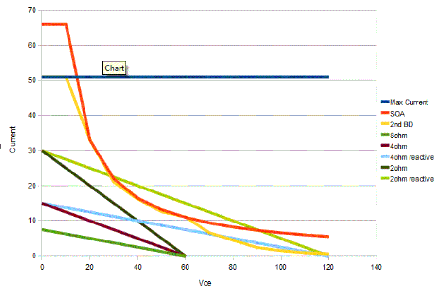
The only line on the graph that is a bit of guess work is the secondary breakdown. I had to read off of a graph on the transistor data-sheet, so it is open to slight error, although it looks decent enough.
From my perspective three pairs looks okay, especially if I use a dual slope protection circuit. However heat this all up so the junction temps = 75 degrees and things fall a bit apart and we get this...
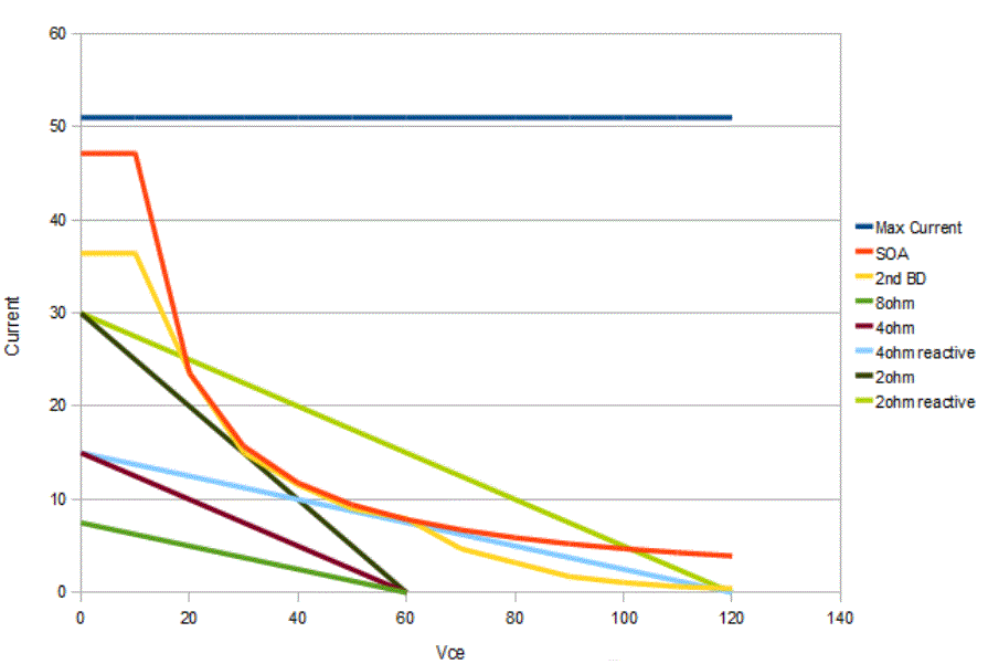
It's not bad for the purely resistive loads, even just about handling 2 ohms. However in the real world purely resistive loads simply don't happen. I'd be happy for this to be somewhat capable into a 4 ohm reactive load and three pairs won't cut it.
Upping this to four pairs we get...
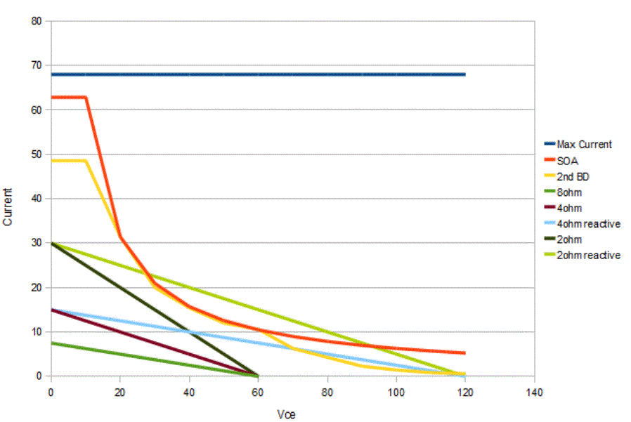
..which to me looks a lot more acceptable.
If anyone thinks three pairs would be enough they are welcome to comment.
Next up is the input stage.
This seems rather easy to get right. The theory I've read says that upping the current source to around 7mA should be enough for this design. Current mirror, emitter resistors and LTP degenerators will obviously be changed.
Self and Slone seem to indicate that having a voltage drop of around 60mV across the current mirror emitter resistors is a nice figure to aim for. This would = having about a 20ohm resistor in this position.
The LTP degeneration I'm not 100% sure about, but simulating shows having this around 33ohms delivers nice performance. I can obviously change this around when the amp's built, if I need to tweak things. In fact that's one thing I am considering doing. Building one and measuring reality to optimise the design.
The VAS. First and foremost the activation point of the transistor that protects the VAS needs to be changed. I've played around with this in the simulator and can appreciate how this works.
In the previous amp design it was recommended that I split the 47R resistor at position R22 into two separate resistors. By altering the values of these I can alter the activation point of the VAS protection. It was also mentioned that altering the value of R22 would change the degeneration of the VAS so again is open to tweaking. In simulation, keeping this at around 47R shows good results, so I plan to start from there.
I am not 100% sure how much current the VAS will require to work effectively. This doesn't appear to be discussed very much and I guess this is because the absolute amounts are determined by the output stage, it's configuration and how many output pairs there are.
To start with I was thinking of setting the VAS current source to around 12mA and going from there.
The protection circuit for the output stage will have to be redesigned, but that's something I'm interested in trying out.
The amplifier currently uses a CFP output stage, something that I quite like as it keeps the quiescent current low, reducing the total current draw when the amp's doing nothing.
When adding multiple output devices, both Self and Slone show one common RE resistor that all the collectors of the output transistors connect to. I am assuming that I can actually split this up and have an RE resistor per collector if it makes the PCB layout easier. Is this so?
I am also going to add catching/clamping diodes to the amplifier, as one of the things I can see them powering presents a highly inductive load.
Are there any other big things I should watch out for? Final component values can be modified after the amplifier has been constructed, but if this is a situation where something like a VAS buffer would be an excellent idea, then I'm all for including it in the design.
Output triples also seem something that might be interesting, but everything relating to them seems rather blurry. Some people say don't use them, they shouldn't be needed and simply make the amp more prone to instablity. And others seem to imply that you wont achieve good performance, in a high power design, unless you've got a triple output stage.
As usual many thanks in advance for any advice anyone might like to add
The temptation to create a higher powered version of the Blameless has got the better of me and I started simulating.
First of all the output stage will obviously require an overhaul. One pair might do it for you if you're goal is to create something resembling a fireworks display. Sadly this would be an irreversible event - if I want fireworks and fine sound maybe I'd be better off with one of these - however I'm not sure how good that would actually sound in practise
I was thinking of using 3 or 4 pairs of these. They look like a relatively new part and the specs look good too, also the price is nice.
Taking a page out of Self's book, I created a spread sheet for looking into device power etc. The SOA line represents the 220 watt max power the device can handle.
Three pairs looks like this.
The only line on the graph that is a bit of guess work is the secondary breakdown. I had to read off of a graph on the transistor data-sheet, so it is open to slight error, although it looks decent enough.
From my perspective three pairs looks okay, especially if I use a dual slope protection circuit. However heat this all up so the junction temps = 75 degrees and things fall a bit apart and we get this...
It's not bad for the purely resistive loads, even just about handling 2 ohms. However in the real world purely resistive loads simply don't happen. I'd be happy for this to be somewhat capable into a 4 ohm reactive load and three pairs won't cut it.
Upping this to four pairs we get...
..which to me looks a lot more acceptable.
If anyone thinks three pairs would be enough they are welcome to comment.
Next up is the input stage.
This seems rather easy to get right. The theory I've read says that upping the current source to around 7mA should be enough for this design. Current mirror, emitter resistors and LTP degenerators will obviously be changed.
Self and Slone seem to indicate that having a voltage drop of around 60mV across the current mirror emitter resistors is a nice figure to aim for. This would = having about a 20ohm resistor in this position.
The LTP degeneration I'm not 100% sure about, but simulating shows having this around 33ohms delivers nice performance. I can obviously change this around when the amp's built, if I need to tweak things. In fact that's one thing I am considering doing. Building one and measuring reality to optimise the design.
The VAS. First and foremost the activation point of the transistor that protects the VAS needs to be changed. I've played around with this in the simulator and can appreciate how this works.
In the previous amp design it was recommended that I split the 47R resistor at position R22 into two separate resistors. By altering the values of these I can alter the activation point of the VAS protection. It was also mentioned that altering the value of R22 would change the degeneration of the VAS so again is open to tweaking. In simulation, keeping this at around 47R shows good results, so I plan to start from there.
I am not 100% sure how much current the VAS will require to work effectively. This doesn't appear to be discussed very much and I guess this is because the absolute amounts are determined by the output stage, it's configuration and how many output pairs there are.
To start with I was thinking of setting the VAS current source to around 12mA and going from there.
The protection circuit for the output stage will have to be redesigned, but that's something I'm interested in trying out.
The amplifier currently uses a CFP output stage, something that I quite like as it keeps the quiescent current low, reducing the total current draw when the amp's doing nothing.
When adding multiple output devices, both Self and Slone show one common RE resistor that all the collectors of the output transistors connect to. I am assuming that I can actually split this up and have an RE resistor per collector if it makes the PCB layout easier. Is this so?
I am also going to add catching/clamping diodes to the amplifier, as one of the things I can see them powering presents a highly inductive load.
Are there any other big things I should watch out for? Final component values can be modified after the amplifier has been constructed, but if this is a situation where something like a VAS buffer would be an excellent idea, then I'm all for including it in the design.
Output triples also seem something that might be interesting, but everything relating to them seems rather blurry. Some people say don't use them, they shouldn't be needed and simply make the amp more prone to instablity. And others seem to imply that you wont achieve good performance, in a high power design, unless you've got a triple output stage.
As usual many thanks in advance for any advice anyone might like to add
The more transistors used in cascade the less stable the amplifier is. I agree with avoiding triples. Triples are unnecessary these days with all the high beta power transistors available. On Semi makes a number of good choices of power transistors in their Sustained Beta series. The On Semi Sustained Beta I use have a minimum beta of 75 and On semi matches them to 10%. With a beta of 75 you can use a small high gain driver transistor like the KSA1220 and KSC2690. These drivers have a minimum beta of 35 and if you were to arrange these transistors in darlington emitter follower topology,then the gain will be 35 x 75 = 2625 minimum. That means, for example delivering 10 A to the load, the worst case current demand on the VAS stage will be 3.81 mA. The beta using CFP will be slightly less that darlington. As for paralleling output transistors, yes you can use individual emitter coupling resistors. I have never seem a pro amp that doesn't do it this way. I have found no advantage of using a single coupling resistor in all the simulation I've done on various output stages.
I find I get better stabllity from what I've described here using emitter follower darlington configuration and paralleling the power transistors. Being able to use a small driver transistor means you can select one with a relatively small COB.
That's not necessarily possible when using the CFP because the current demands on the driver transistor are far greater with CFP. That means you will have to use a larger driver transistor and therefore the COB will be larger. The more capacitance you have (COB) in the VAS, driver and output stage the harder it is to stablize and compensate the amplifier. With more COB you be forced to use larger amount of miller capacitance for compensation and that limits the bandwidth and effects the slew rate of the amplifier.
Hope this helps.
David.
When adding multiple output devices, both Self and Slone show one common RE resistor that all the collectors of the output transistors connect to. I am assuming that I can actually split this up and have an RE resistor per collector if it makes the PCB layout easier. Is this so?
This is not possible if you wish to keep the same topology. I have used three output pairs, and included separate emitter resistors, which Self did not use in his 2-pair example. I found this puzzling. I my application I paralleled two 0.22R 0.5watt resistors per output device, which saves some space.
"I agree with avoiding triples. Triples are unnecessary these days with all the high beta power transistors available. On Semi makes a number of good choices of power transistors in their Sustained Beta series."
David, if your load is 8 Ohms resistive, then this may well hold. However, real world loads are much tougher (VI phase specifically and Rl as low as 3 Ohms, sometimes 2 Ohms). Distortion rises dramatically into these lower loads as the load is reflected back into the VAS.
In terms of instability in the triple output stage, there are a few simple techniqies to overcome this -the simplest is the use of base stoppers, while another is an RC network in the base of the drivers.
As an example, I am currently running my amp (280W into 8 ohm, 500W into 4) using BF472 predivers, MJ15032/33 drivers followed by the output devices. I am using an RC network on the driver base for stability. This is a low feedback design, and so benefits enourmously from the use of a triple output topology ('Locanthi 'T'). I am running both the pre-driver and driver stages heavily in pure class A into 2 ohm output load.
Regards
"David, if your load is 8 Ohms resistive, then this may well hold. However, real world loads are much tougher (VI phase specifically and Rl as low as 3 Ohms, sometimes 2 Ohms). Distortion rises dramatically into these lower loads as the load is reflected back into the VAS.".
When I hear the word triples I'm thinking it means triple darlington. Are we talking about the same thing here. My amplifier is stable down to a 2 ohms reactive load but is intended to operate at 8 ohms 100w, albeit with a slightly higher distortion at 2 ohms.
I am well aware of the conditions you mentioned.
David.
When I hear the word triples I'm thinking it means triple darlington. Are we talking about the same thing here.
I am not sure. Yes and no I think, it depends on what configuration you're after.
Self has a triple EF in one of this schematics for a triple configured output stage. But he also has two others that he calls an EF-CFP output stage and another that he calls a CFP-EF output stage.
The first where the pre and pre pre drivers are configured as an EF, with the pre drivers and output transistors configured as a CFP.
The second where the pre and pre pre drivers are CFP and the pre driver and output stage are EF.
All three attempting to address the same issue, but in slightly different ways.
I found this puzzling. I my application I paralleled two 0.22R 0.5watt resistors per output device, which saves some space.
Yes, that is puzzling, the load invariant doesn't have any emitter resistors. I was under the impression that these are to ensure equal current sharing between the output transistors. And in a CFP output stage the RE resistors that go from the collector to the output are simply there to work the protection circuitry.
I am not sure. Yes and no I think, it depends on what configuration you're after.
Self has a triple EF in one of this schematics for a triple configured output stage. But he also has two others that he calls an EF-CFP output stage and another that he calls a CFP-EF output stage.
The first where the pre and pre pre drivers are configured as an EF, with the pre drivers and output transistors configured as a CFP.
The second where the pre and pre pre drivers are CFP and the pre driver and output stage are EF.
All three attempting to address the same issue, but in slightly different ways.
It's been a while since I read self's book. I do believe though he said the reason for triples is because if one uses lower gain output transistor and one is paralleling many of them then it may be necessary to use triples to get the gain up. That may have been true back in the late 70s and early 80s when high gain power transistor were not available, but they are today and so if we use high gain output then triples are not necessary and you will have a more stable configuration.
In the twenty years I spent repairing pro amplifiers as well as HiFi and high end audio power amplifiers, I have not seen triples used very much and the ones that did blew up a lot more often. I have seen every mistake a engineer could make in the design of power amplifier. It's been my experience that the more I have to compensate an amplifier for stability, the more it takes away from the performance of the amplifier in some way.
But maybe you guys have some better tricks for stabilizing an amplifier than I do.
David.
I have built this one. In retrospect I have to call it a learning amp, as I have learned some lessons with this one. The component values are pretty much what is in the Amp right now. But I would make some changes (also in topology) in the next redesign.
Directupload.net - D26rb9ct7.png
Having a look at the outputstage I would consider this a buffered VAS driving a CFP. This does not seem to fall under the pure triplet definition Self uses, so I found it worth mentioning.
I have had some issues with the stability, but they were rather mild in charachter - nothing blew up.
I found (by ear) quite an improvement in high frequency reproduction as I increased the output bias from 5mV to 20mV. I don't know what to blame, maybe this configuration has a different optimal bias than the pure CFP, maybe it was not entirely stable with the lower bias.
This expirience lead me to the conclusion to try the standard EF (still triple though) type outputstage next time, or use lower emitter resistance (than 0.22R) with the CFP for more standing current.
A lot of speculation in that last part. Sorry if it is more confusing than helping.
I have built this one. In retrospect I have to call it a learning amp, as I have learned some lessons with this one. The component values are pretty much what is in the Amp right now. But I would make some changes (also in topology) in the next redesign.
Directupload.net - D26rb9ct7.png
Having a look at the outputstage I would consider this a buffered VAS driving a CFP. This does not seem to fall under the pure triplet definition Self uses, so I found it worth mentioning.
I have had some issues with the stability, but they were rather mild in charachter - nothing blew up.
I found (by ear) quite an improvement in high frequency reproduction as I increased the output bias from 5mV to 20mV. I don't know what to blame, maybe this configuration has a different optimal bias than the pure CFP, maybe it was not entirely stable with the lower bias.
This expirience lead me to the conclusion to try the standard EF (still triple though) type outputstage next time, or use lower emitter resistance (than 0.22R) with the CFP for more standing current.
A lot of speculation in that last part. Sorry if it is more confusing than helping.
CFPs are more difficult to compensate but are more thermally stable. EFs are more stable compensation wise but are less thermally stable. Using a triple darlington configuration increases the problem with thermal stability. Self talks about this in his book. However a really big heat sink will probably fix the problem. Thermal instability in darlintons is caused from an ever increasing gain with an increase in temperature. This thermal instability with EFs causes the standing current to keep increasing until we have a condition called thermal runaway or just simply smoke. The emitter coupling resistors help to dissipate some of the energy, but offer only a marginal amount to the thermal stability of the output stage.
David.
I agree with bonsai on this, triples give excellent performance and are not too hard to compensate, with a well designed Vbe multiplier theres no problems with thermal runaway, inadequate design will lead to some problems. My second choice would be a cfp prediver followed by a EF which also offers a big improvement over the typical Self EF design.
I agree with bonsai on this, triples give excellent performance and are not too hard to compensate, with a well designed Vbe multiplier theres no problems with thermal runaway, inadequate design will lead to some problems. My second choice would be a cfp prediver followed by a EF which also offers a big improvement over the typical Self EF design.
Ok then can one or both of you post some examples on stabilizing this circuit.
Amcron used triples in a number of there designs. They used a 470Pf in parallel with a small inductor placed between the predriver and driver or maybe it was before the predriver transistors it's been a long time since I repaired one. I had a lot of there amps land on my bench.
David.
Probably inadequate design, nearly all rotel amps use triples dating back to the 1980 s, marantz uses them in their top of the range and so do many other brands and no caps or inductors are needed, thats why they most probably failed often, study rotel or marantz schematics, they designed them appropriatly. Transistor selection and layout is of prime importance. I could even show you well respected pro amps using triples. You can even get away with using no output coil like marantz and rotel do. I have a couple of rotels, one is 17 years old uses no output coil and has never had any problems, I used them to drive my BW804 s for a while.
I dont think I should place a schematic of a rotel or marantz here, but I could email you one, how about one of their top of the range and currently on sale amps. I dont use BJT output s in my triples anymore but mosfets and I find them even easier to stabilize.
I dont think I should place a schematic of a rotel or marantz here, but I could email you one, how about one of their top of the range and currently on sale amps. I dont use BJT output s in my triples anymore but mosfets and I find them even easier to stabilize.
I don't want to give my primary address here so send them to davada50@gmail.com from there I'll give you my primary address.
I hope we are not hijacking this thread.
Is this ok 5Th Element?
Oh this isn't thread jacking, it's entirely relevant to what I am trying to do and it's interesting. So please do not stop on my account, in fact do carry on
. I am going to try one board without triples and see how that fares. If the design clearly isn't happy, I'll probably try a board with triples.
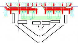
Anything relating to board layout, even if just small tips would be appreciated. The PCBs I designed for the 80-100 watt design were a success and in no small part because of Self's guide. However I'm presuming that there are certain tracks that should be kept short and possibly kept away from 'things' to ensure stability. If I can incorporate them now, that'd be rather handy.
Naturally I am trying to keep things compact and by doing so reduce trace length, but there are limits to these things. For example however.
This is the first edition of the PCB, where I simply connected the output transistors together. I can move them slightly closer in to reduce trace length a little, either way, cue my MS paint skills.
What we've got marked are ideas for the pre driver locations.
A) would keep the pre drivers close together.
B) would place them further apart, but put them slightly closer to the output stage.
C) C over position B, moves them even further apart and would perhaps minimise trace length a little bit, between the pre-drivers and the output transistors, .
From what I understand increasing the distance between the two pre-drivers shouldn't be of any concern. What is important though is keeping the trace length between the pre drivers and their relative output transistors to a minimum - as it's the pre driver + output transistors that form the functional 'part' of the amplifier.
Attachments
Just violate all RF rules for board lay out.
Most important as Self pointed out is to take the feedback point on the board right from the output where you speaker wire will connect.
If the traces are wide then the length is not such a big issue. You want to keep the trace resistance as low a possible. Grounding is a big big issue. Have everything wired to a central ground point down stream from the reservoir caps. Not necessarily on the board. Keep you input ground separate from rail bypassing caps ground returns. Place you input ground down stream from other heavy current grounds like the speaker ground. The idea is to keep the grounds as close to the same potential as possible. never loop a ground or a power rail for that matter. I've seen people do that on their boards.
- Status
- This old topic is closed. If you want to reopen this topic, contact a moderator using the "Report Post" button.
- Home
- Amplifiers
- Solid State
- Beefing up the Blameless.