Well, for what it's worth..... here it is.
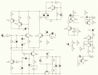
This is just the main pcb and does not include output stage, psu etc.
It is messy and of unconventional layout as it was hand drawn by myself many years ago whilst reverse engineering it to enable a repair. All the "wires" that seem to just abruptly end and go nowhere are where they leave the board and go to the rest of the amp.....
Perhaps someone would care to redraw the rats nest of a schematic so it is more easy to read and understand?
From what I recall, there is nothing special about the output stage and it is just a set of the output transistors (used as drivers and on the same heatsinks) driving paralleled sets of the same type transistors (4 each of pnp and npn per channel I think) in a darlington type arrangement.
I have no other information.
Attachments
Will someone suggest a appropriate computer program that will BEST make the schematic with? I want it to be as good as I can make it. I have redrawn it by hand and assigned part numbers, but I want to enter it into a computer drafting and or CAD system...
There is one for sale on ebay, it has some very detailed Pictures. the price is starting at about 200 with shipping, I would like to get it but the cost is beyond me today...
Thanks for your help.
There is one for sale on ebay, it has some very detailed Pictures. the price is starting at about 200 with shipping, I would like to get it but the cost is beyond me today...
Thanks for your help.
Last edited:
- Status
- This old topic is closed. If you want to reopen this topic, contact a moderator using the "Report Post" button.
- Home
- Amplifiers
- Solid State
- Dunlap Clarke schematic as promised.