hello,
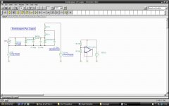
attached you will find a .zip file containing three amplifiers, only differing in the vertical MOSFET output pair biasing arrangement :
- Class AB,
- Class AB Non-Switching,
- Class AB Soft Non-Switching
The three files are Tina 7 Texas Instruments schematics ready for simulation.
Are you equipped with Tina 7 Texas Instruments ?
Have you read the subject till the end ?
May I suggest that you post here, only if you satisfy the two conditions ?
1.
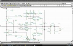
The Class AB arrangement is a fixed voltage Vbe multiplier, decoupled by a big capacitor in parallel, as usual.
2.
The Class AB Non-Switching arrangement samples the 0,47 ohm source resistor voltage drop of both MOSFETs, individually, and compares the voltage drop with a reference voltage. When the 0,47 ohm resistor voltage drop is less than the reference voltage, the non-switching arrangement sends a correction current into the base of the Vbe multiplier that's associated to the MOSFET. Both MOSFETs thus never go off. However cumbersome or complicated it sounds, it works on paper (on simulation).
3.
The Class AB Soft Non-Switching arangement bias servo-loop is now getting a variable loop gain. The loop gain is minimized when the instantaneous 0,47 ohm current is minimal. The trick is in the differential amplifier operating current. It is now variable so the dynamic Rbe varies accordingly (log relation), and come in series with the 180 ohm emitter resistors. The 180 ohm resistors define the maximal loop gain, when the dynamic Rbe become small in front of 180 ohm.
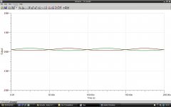
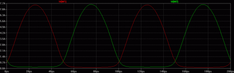
The waveforms look perfect with a 1KHz 500 mV signal at the input. There are no hard corners nor inflexions anymore in the MOSFETs source currents. All the edges are nicely softened. When viewed from a certain distance, this may be confused with smooth genuine Class-A operation.
***
However, inputting a 500mV 10 KHz sinus signal enables us to see that :
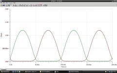
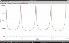
- The Class AB arrangement delivers the cleanest MOSFETs source currents in the changeover zone, but the current drops to zero, and there are hard corners in the changeover zone, meaning a strong high-frequency harmonic content, internally. That's not new. This is known from long, and is the specificity (and flip side) of Class AB operation.
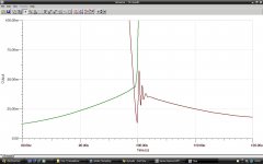
- The Class AB Non-Switching arrangement manages to keep both MOSFETs in conduction, but is prone to HF micro-oscillations bursts (1 Mhz, 2 µS duration, 25 millivolts amplitude), very localized inside the changeover zone. Apart from the HF bursts, there are hard corners in the changeover zone, meaning a strong high-frequency harmonic content, internally.
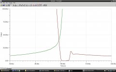
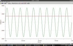
- The Class AB Soft Non-Switching arrangement manages to keep both MOSFETs in conduction, and is delivering smooth rounded current edges, without harsh harmonic content. When looking closely, one can see that the Soft Non-Switching arrangement is perfectly working on the leading edges, when the MOSFETs currents go from low quiecent current to high load current. However, both MOSFETs do experience a small 5 µs duration, 10 millivolts ampitude glitch at each trailing edge, when the MOSFETs currents need to go from high load current to low quiecent current. The wavevorm that I am publising is the extreme version of the glitch, when the output delivers a 80 Volt peak-peak 10 KHz sinus, and causing a very brief zero current.
I have selected this worst-case waveform ON PURPOSE in order to ask the diyAudio communauty "hello, can someboby help me ironing-out this glitch ?".
Any suggestion welcome,
Steph
attached you will find a .zip file containing three amplifiers, only differing in the vertical MOSFET output pair biasing arrangement :
- Class AB,
- Class AB Non-Switching,
- Class AB Soft Non-Switching
The three files are Tina 7 Texas Instruments schematics ready for simulation.
Are you equipped with Tina 7 Texas Instruments ?
Have you read the subject till the end ?
May I suggest that you post here, only if you satisfy the two conditions ?
1.
The Class AB arrangement is a fixed voltage Vbe multiplier, decoupled by a big capacitor in parallel, as usual.
2.
The Class AB Non-Switching arrangement samples the 0,47 ohm source resistor voltage drop of both MOSFETs, individually, and compares the voltage drop with a reference voltage. When the 0,47 ohm resistor voltage drop is less than the reference voltage, the non-switching arrangement sends a correction current into the base of the Vbe multiplier that's associated to the MOSFET. Both MOSFETs thus never go off. However cumbersome or complicated it sounds, it works on paper (on simulation).
3.
The Class AB Soft Non-Switching arangement bias servo-loop is now getting a variable loop gain. The loop gain is minimized when the instantaneous 0,47 ohm current is minimal. The trick is in the differential amplifier operating current. It is now variable so the dynamic Rbe varies accordingly (log relation), and come in series with the 180 ohm emitter resistors. The 180 ohm resistors define the maximal loop gain, when the dynamic Rbe become small in front of 180 ohm.
The waveforms look perfect with a 1KHz 500 mV signal at the input. There are no hard corners nor inflexions anymore in the MOSFETs source currents. All the edges are nicely softened. When viewed from a certain distance, this may be confused with smooth genuine Class-A operation.
***
However, inputting a 500mV 10 KHz sinus signal enables us to see that :
- The Class AB arrangement delivers the cleanest MOSFETs source currents in the changeover zone, but the current drops to zero, and there are hard corners in the changeover zone, meaning a strong high-frequency harmonic content, internally. That's not new. This is known from long, and is the specificity (and flip side) of Class AB operation.
- The Class AB Non-Switching arrangement manages to keep both MOSFETs in conduction, but is prone to HF micro-oscillations bursts (1 Mhz, 2 µS duration, 25 millivolts amplitude), very localized inside the changeover zone. Apart from the HF bursts, there are hard corners in the changeover zone, meaning a strong high-frequency harmonic content, internally.
- The Class AB Soft Non-Switching arrangement manages to keep both MOSFETs in conduction, and is delivering smooth rounded current edges, without harsh harmonic content. When looking closely, one can see that the Soft Non-Switching arrangement is perfectly working on the leading edges, when the MOSFETs currents go from low quiecent current to high load current. However, both MOSFETs do experience a small 5 µs duration, 10 millivolts ampitude glitch at each trailing edge, when the MOSFETs currents need to go from high load current to low quiecent current. The wavevorm that I am publising is the extreme version of the glitch, when the output delivers a 80 Volt peak-peak 10 KHz sinus, and causing a very brief zero current.
I have selected this worst-case waveform ON PURPOSE in order to ask the diyAudio communauty "hello, can someboby help me ironing-out this glitch ?".
Any suggestion welcome,
Steph
Attachments
-
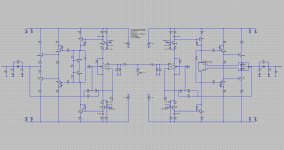
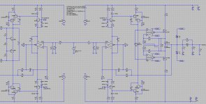
 Sansui Diamond-Differential with current mirror loads and self biased VAS cascodes and Non-Switc.jpg100.6 KB · Views: 1,592
 -
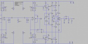
 Sansui Diamond-Differential with current mirror loads and self biased VAS cascodes and Soft Non-.jpg99 KB · Views: 1,558
 -
Class AB, Non Switching Class AB, Soft Non Switching Class AB.zip624.1 KB · Views: 446
Both curves are the voltage drop on the 0,47 ohm resistor (source resistors). Have you conducted some simulations yet ? Are you now able to reproduce the curves ?Looks like tail current of one of the driver transistors ?
Interesting question. If one of the drivers transistors shuts off, maybe one of the Vbe multiplier endures a zero current, with the Vbe multiplier voltage vanishing. That's a direction to be investigated, indeed ! However, do you think this is occuring with a 10 KHz sine ?Are any drive transistors allowed to shut off ?
Since I don't happen to be using Tina, could you provide
all three schematics as Jpegs?

Didnt you try to open his zip files?...One never know....
Last edited:
I don't fully understand the circuit yet, but looks like tail current of one
of the driver transistors? Are any drive transistors allowed to shut off?
Good point. I was looking at it from another angle. The soft-non-switching circuit has to handle a very non-linear high-dynamic range across that 0.47ohms. If you look at the circuit, it's ingenious but involved. The feedback loop back to the Vbe multiplier has non-linearity and phase shift, and inho that is the cause for the small damped oscillations when the output device currents are going down to zero. That loop not only includes the regulation circuit but also the Vbe multiplier, drivers and output devices with wildly differing dynamic properties.
It's a matter of getting that loop stable and it is solved.
In a more philosophical sense, in my experience, trying to control the bias current with a closed loop almost always brings up two issues: loop stability, and/or bias modulation by the signal due to the high dynamic range of the Re voltage.
jd
Last edited:
hello dear friends,
thanks for your interest in this novel amplification sub-class. By the way, is this really a "novel" amplification sub-class ?
It may be ...
I know there is a lot of litterature about servo-controlling the minimum bias current in the output devices of power amplifiers, and I know some practical circuits materializing this.
However, I could not find litterature about doing this in a well controlled, smooth and soft approach, minimizing high-frequency generation within the circuit. And I never came across a practical circuit materializing this smooth and soft approach.
Anyway, being the inventor or not of the Class AB Soft Non-Switching amplification sub-class, I'm now offering you an improved schematic. This new release manages to get both MOSFETs delivering smooth current waveforms. This time there are no glitches, no hard corners, and no high-frequency contents anymore. I managed to iron-out everything by adding a few simple components from my previous version delivered in this thread. The positive current now blends admirably smooth with the negative current during the crossover.
Truly amazing ... on simulation.
Class AB Soft Non-Switching now exists ... on simulation.
Have fun playing with the attached .zip containing the Tina 7 T.I. circuit ready for simulation.
Any candidate for evaluating the (novel ?) Class AB Soft Non-Switching schematic in the lab ?
Attachments
-
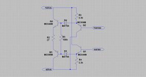
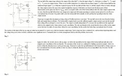
 Class AB Soft Non-Switching (circuit).jpg219.4 KB · Views: 1,482
 -
 Class AB Soft Non-Switching (0.47R voltages - 4Vpp out).jpg94.1 KB · Views: 1,406
 -
 Class AB Soft Non-Switching (0.47R voltages - 40Vpp out).jpg111.2 KB · Views: 1,295
 -
 Class AB Soft Non-Switching (0.47R voltages - 40Vpp out - zoom).jpg108 KB · Views: 302
 -
Sansui Diamond-Differential with current mirror loads and self biased VAS cascodes and Soft Non-.zip8.1 KB · Views: 191
I too been scratchin to figure, "what is this amplifier class?"
Are we perhaps working different paths to the same end result?
My curves look just like yours, but derived by entirely different
method and circuit. (See: Visch or not to Visch thread)...
Compare to 3rd Screenshot of Post#7 above.
Are we perhaps working different paths to the same end result?
My curves look just like yours, but derived by entirely different
method and circuit. (See: Visch or not to Visch thread)...
Compare to 3rd Screenshot of Post#7 above.
Attachments
What about the + and -15V auxiliary power supplies that are needed, centered on the output of the amplifier ? Weird stuff ... horribly expensive and cumbersome ? Maybe not ...
I remember some time ago Jan Didden's PAX amplifier in Elektor. PAX needs two 15V power supplies centered on the amplifier's output for powering a AD844 IC. PAX elegant circuit relies on two bootstrap capacitors feeding two 15 V zener voltage stabilizers.
I have used the same layout. However, conducting some extreme simulations (like 10 Hz audio signal near clipping), I found that some non-sinus ripple was developing using a single zener layout.
A proper tradeoff needs to be found : fast recharging speed (low value charging resistances) against low ripple amplitude (high value reservoir caps). Speed is indeed needed for enabling a proper 15V generation even on a single low duration burst near clipping. Percussive music is a sequence of short bursts.
I think it is tolerable to get a small slow-moving sinus modulation on the 15V supplies in some extreme situations. I think it is less tolerable to get small (maybe smaller) non-sinus (charging waves) on the 15V supplies.
In the proposed bootstrap scheme, I have thus raised the voltage up to 18V using a 1st zener, filtered to 15V by a 2nd stage using a 15V 2nd zener. Depending on personal preference, one can can opt for the 2nd stage, or one can drop it.
Anyway, provided one can reasonably tailor the speed/smoothness compromize in extreme situations, the bootstrap scheme provides an elegant solution to the requirement of + and -15V supplies centered on the output.
One may argue that it draws current, non sinusoïdal current maybe, from the output of the amplifier. Well, with bootstrap resistors equal to 1K, the bootstrap current is confined to small values. I won't say this is neglectible, but I will say it is reasonable.
Are audiophile people rejecting this elegant bootstrap scheme ?
Are there other solutions, really ?
In the attached files, there is a Tina 7 T.I. schematic ready for simulation.
Cheers,
Steph
Attachments
What about the + and -15V auxiliary power supplies that are needed, centered on the output of the amplifier ? Weird stuff ... horribly expensive and cumbersome ?
Are there other solutions, really ?
Well, you could abuse a pair of isolated 15V wall warts...
But then again, I got a much simpler alternative output
stage doin basically the same thing, with only one wart.
And its ref'd to the top rail, don't have to float with the
output... I'm still trying to figure out a no wart solution.
hi kenpeter, that's truly amazing. Yes indeed, we are both in search, exactly at the same time, of a proper implementation for a Class AB Soft Non-Switching amplifier ! Your implementation is very interesting, because of using two N-MOSFETs which means that any DMOS process can integrate the arrangement into a IC, like a TDA7293.My curves look just like yours, but derived by entirely different method and circuit. See http://www.diyaudio.com/forums/solid-state/163364-visch-not-visch.html
Compare to 3rd Screenshot of Post#7 above.
Please get a look to this thread : http://www.diyaudio.com/forums/solid-state/162644-siliconix-siemens-nmos-amplifiers.html
Would be fantastic to show us how the famous and mis-estimated Siemens BUZ20 amp can be turned into a proper Class AB Soft Non-Switching amplifier.
Truly I believe that the Class AB Soft Non-Switching amplifier, integrated on a IC and embedding two strong vertical NMOS (aka TDA7293) or strong BJTs (LM3886), is the only alternative in the long run, to Class D amps.
However, linear ICs like TDA7293 and LM3886 are going to stay limited in power, unless they offer the required dissipating surface. On top of that, some audiophile people will say that getting an input stage working on Monday at 45° centigrade, and working on Saturday night at 85° degree centigrade, is definitely not a quality-insurance for sound.
Some audiophiles are going to want the same schemes than the yet to be announced Class AB Soft Non-Switching amplifiers in ICs. Some audiophiles (or many ?) will want to implement the Class AB Soft Non-Switching using discrete components.
It they can't, they'll be very sad.
The irreductibles will need Peltier-thermoregulated dual JFET front-ends, claiming this is the only way to get low noise and stability. Am I Joking ? Maybe not, as the Peltier may surround the dual JFET front-end, same die. This, also, within a linear audio power amplifier IC. Linear audio power amplifiers ICs may still surprise us in a possible future ... Competing with them using discretes is going to be tough ..
Have fun,
Steph
My power devices are strongly controlled by local feedback
and not operating to their own native curve. Maybe yours
are doing something similar?
If so, then it hardly matters if the devices used are good
compliments, as long as the strong control circuitry holds
the complimentary curves. You might turn this fact to
your advantage? I'm thinking of changing my top MOSFET
for an NPN, to help get rid my last remaining bootstrap.
That's your choice ... but that's weird. In industry, people prefear a step-by-step approach, leading to safe incremental changes. As we are both in search of implementations of Class AB Soft Non-Switching amps, one may categorize the way research and experimentation gets conducted :I'm thinking of changing my top MOSFET
for an NPN, to help get rid my last remaining bootstrap.
- starting from a kind of "blameless" amp (however Full Symetric, Mr Self, and having some current feedback genom inside for improved slew-rate), well understood by the industry, and then, based on this, design a Class AB Soft Non-Switching add-on. You'll recognize my approach there. It leads to heavy circuitry (as a disadvantage), but it is easy to model, easy to understand, and easy to integrate into an IC, and easy to derive as a small SMD bias controlling add-on board for the DIY market.
-starting from the famous Siemens BUZ20 amp (Etienne Lemery proven implementation), and see how the two vertical N-MOS can be persuaded to work Class AB Soft Non-Switching. It's quite late here, I need some sleep, and I still need to see if this is your approach. If I were you I would use without hesitation one or two boostraps for getting a drive above the main power supplies. Bootstraps are used everywhere now where it is question of efficiently driving vertical MOSFETs. Read the TDA7293 datasheet with attention.
- starting from the "industry standard" TDA7293 amp and see how the two vertical N-MOS can be persuaded to work Class AB Soft Non-Switching.
- starting from the other "industry standard" LM3886 amp and follow the same path as for the TDA7293. At this moment I have no info about the internals of the LM3886.
- getting something completely new, kind of revolution, where you can't recognize anything from the past. It is very important to characterize them like if you know nothing about beforehand, and torture them 1000 different ways. One should remember they are based on no known expertize. Surprises may arise : latchup, HF susceptibility, phase inversion on overload, gaps in the capacitive load tolerance, ... If properly designed and tested, this approach may deliver the highest quality / complication ratio.
Those are the main directions IMO, and they are not competing. It is a matter of getting the Class AB Soft Non-Switching technique mature, in a structured way, not confusing the principle with the various implementations to be found, rediscovered, or invented.
Cheers,
Steph
Last edited:
hello, in one month time I have switched to LTspiceIV for the simulations, and derived a Kenpeter solution using a simple but accurate soft non-switching controller, sampling the current using two Schottky diodes plus one common parallel resistor.
The whole amp is based on the Kuroda 1982 amp, but this time with a BJT complementary Darlington at the output.
Such amp is a flexible development platform. Using the same simple PCB, it is now possible to test :
- various opamps as front-end
- biasing the output devices using a dumb Vbe multiplier (capacitor bypassed or not)
- biasing the output devices using a Edwin scheme (a small Class A embedded into a class B)
- feedforward error correction using the Quad 405 / Sansui Feedforward scheme (a small Class A embedded into a class B, with a RCRL bridge)
- various non-switching bias controllers like Technics New Class A, JVC Super-A, Pioneer NSA, Sansui Non-Switching, Hitachi Super-Linear... and Kenpeter.
See attached .zip
The best results are obtained using the schematic #3.
Cheers
Steph
Attachments
Member
Joined 2009
Paid Member
When I get home from testing (and if necessary
troubleshooting) 150-200 class D amps and/or
other EVMs per day. Build an amp? Its a bit too
much like my workday. Ok, maybe something w.
tubes and no USB/I2C/I2S wouldn't be entirely
like work...
Playing with LTSpice just how I give myself a break
while still plausibly at the same time doing my job.
Even thats getting harder to squeeze by the critics.
They now prefer I play with LABVIEW if I gotta act
all ADD while doing the more mind-numbing of the
repetitive plug, and click, and measure, and unplug
testings...
They did pay for a lot of Labview training I havn't
put to much good use yet. All this GPIB stuff, its
just faster tweakin' front panels than wait for a PC.
I fought with NI-VISA today and lost. Need to put
all this NI carp on a clean PC, so's versions match.
Too many conflicting runtimes from all the other
old and new test procedures I have to switch
softwares and drivers and gut the registry every
other day.
You guys build it. Let me know how it goes.
I may chime in with an idea if anything burns
through the tinfoil hat. Real tin, accept no
substitutes!
One of these days I'm gonna call in sick with
George Jetson's disease. Don't wanna push that
darn button no more... My mouse finger could
probably swing a blacksmith's hammer by now
if not for the arthritus.
Last edited:
hello, in one month time I have switched to LTspiceIV for the simulations, and derived a Kenpeter solution using a simple but accurate soft non-switching controller, sampling the current using two Schottky diodes plus one common parallel resistor.
The whole amp is based on the Kuroda 1982 amp, but this time with a BJT complementary Darlington at the output.
Such amp is a flexible development platform. Using the same simple PCB, it is now possible to test :
[snip]Steph
Steph,
Very interesting! Such an universal amp platform is something I like a lot to play with. Very curious as to your findings.
BTW, you motivate me to also switch to LTspice. If I only can find the time...
jd
hello,
and I apology in advance for a terribly long post. This week, Paul Kemble - great source of inspiration : check his website on A Paul Kemble web page - index to 'sound' webpages. - pointed a very interesting circuit.
It was in Electronics World, April 1998. See here : Audio Amplifier Circuit Design
This webpage is marked "copyright Renardson". So, let's call this "the Renardson Feedforward" scheme until we know more. It would be interesting to have a .pdf copy of the Electronics World, April 1998 article. Will somebody point a link or post an attachement ?
Getting an ultra-low THD in Class AB with only 12mA quiescent current is remarkable. The idea is to linearize the output stage using local feedback, a smart evolution of the well known bipolar CFB arrangement. The available gain is used in a smarter way than the well known CFP. One can view it as a feedforward scheme, purely applied to the output stage, not involving the VAS in any way. That's brilliant.
I got amazed, but then, looking closer, I got dissapointed by three negative features :
- One of the two output device is the leader (the bottom one), and the other one (the top one), follows the leader and adds value by applying the feedforward correction.
- The current waveforms are asymetric, with the upper device emulating a constant current source most of the time
- The bias current is not rock-solid when a 100% feedforward correction is applied.
However, the idea is great. I wanted to test the idea of using the reserve gain of a BJT CFP arrangement, but this time, fully symetric, linearizing each power BJT in a crossed way, so there is no more a "leader" device and "follower" device.
And, naturally, adding a Soft Non-Switching feature, as this is the theme of the present thread.
Of course, we are not going to play with very low quiescent currents. We will target quiescent currents in the order of 50 mA to 250 mA and see what are the result. See how the circuit crosses, and see what is the guaranteed Non-Switching domain. That's what we want to do.
So, practically, we will add the Soft Non-Switching feature by sampling the voltage on a Schottky stack, basing on Kenpeter work.
I guess that the maths will show that the feedforward distorsion cancellation is not there anymore, as the feedworward is applied on a non-linear element like the Schottky stack.
But anyway, THD is indeed lower than the best Kuroda implementation, and that's not a light statement knowing the performance of the Kuroda. That is thus the first circuit. You'll recognize it easily : there are BJTs at the output. This is the "101" file.
Then I pushed the concept, using a MOSFET output stage, with each output device getting linearized using local feedback (or feedforward ?) in a crossed manner, this time using the available gain of custom-made OpAmp drivers. Looks crazy, but it works. Simulated THD is even lower ... This is the "001" file. Truly amazing.
In the "001" circuit, there is a fiddle regarding the exactness of the feedback. Go back to the "101" circuit, and consider the feedforward differential resistors. They are all equal to 100 ohm, still compliant with the theory of operation of the feedforward arrangement. But here, in a mutual, crossed way.
Now look the "001" circuit. The resistors are now 100 ohm / 290 ohm. Which means that we are losing the exactitude of the feedforward scheme. Is that relevent, now that the arrangement is mutual, and crossed ?
Need to do the maths.
But why not observing the 100 ohm / 100 ohm ratio anymore in circuit "001" ? The answer lies in the bias current instability issue. If, like here, you don't have two BJT junctions to compensate (there are two BJt junctions in version 001), with a 100 ohm / 100 ohm arrangement, meaning a total feedforward arrangement, you end-up with a behaviour like you have an infinite Vbe multiplier. So, as demonstration purpose, I have thus used the lowest stable voltage reference (one BAT54 Schottky drop), and I have then tailored the other resistor for getting a decent idle current in the MOS. This is how the 290 ohm value came. Such arrangement has a rock-solid bias current.
If you want to become closer to a the 100 ohm / 100 ohm ratio, you may use a voltage divider on the BAT54 Schokky used as voltage reference, say divide the voltage by a factor of 5 (say, 50mV), and then, you'll see that for restoring a decent bias current in the MOS, you'll need to use 150 ohm or 120 ohm. But the more you decrease the reference voltage, the more you run the risk that due to offset in the OpAmp drivers, that the bias current will become uncertain. Anyway, you you won't be able to use a 100 ohm / 100 ohm combination, because then, you are supposed to use a zero volt voltage reference, and zero volt is far more than the offset uncertainties of the OpAmp drivers.
May be interesting to embed a Vbe or Schottky offset bias voltage into each OpAmp driver, for having the possibility to use a 100 ohm / 100 ohm ratio in the feedforward arrangement. Don't know if this is feasible.
Now you understand that "001" is still a concept-circuit, instead of something one may build physically. And there is more.
As you can see, there is a bootstrapped +15V -15V power supply, centered on the output of the amplifier. This bootstrapped power supply is needed for powering the custom-made OpAmp drivers. At the moment, the simulation only works fine when using a "battery", instead of a true, real bootstrapped supply. There is the issue.
If you want to waste a full night debugging a LTspice simulation, do like me. Replace the "battery" symbol by the usual bootstrapping capacitor, resistor and zener, and you'll enter the weird world of latchup at power-on, inside the custom-made OpAmp drivers. During power-on, the VAS may evolve randomly with large and brief voltage excursion like -30V, during a the first few microseconds, while the output of the amplifier is still close to zero. You may ask why the amplifier output is still close to zero, while the VAS already started to move randomly. That's normal : the MOSFETs need the OpAmps to be decently powered (like +6V/-6V), before they can follow the VAS in his erratic power-on figure. And remember those OpAmp drivers are not yet on. It is the output of the amp that will provide the supply, through bootstrapping. Now you get the picture. That's a kind of fatal embrace, a deadlock. You then get something very weird : the -30V of the VAS that gets connected to the inputs of the OpAmp drivers, is completely out of the common mode voltage of the Opamp drivers. And guess what : you get tens of milliamps coming out of the OpAmp inputs, as latchup symptom, where normally there would be only tens of microamps. And it is not a temporary glitch. It is a fatal embrace. The OpAmps don't recover. It is a power-on latchup. Your amp doesn't start. It hangs.
Of course I have tried circumventing this by adding timing capacitors at various places, by adding a soft-start feature on the power rails (0.3 ohm serial resistance and 47,000 µF decoupling) but nothing helped. Once you know where to put your current probes (the best place is at the input of the OpAmp drivers), it is amazing to see what's happening during time zero untill something like 500 microseconds. There is a whole revolution taking place inside the amp. You see it on the .TRAN graph. You see the amp waking-up, the VAS starting toggling erratically, getting significant amplitudes after 50 microseconds where the power supply starts delivering more than 10 volt, and then, just when you think that the amp will gentky settle, being now powered with a decent voltage like 30 volt, you see a last random VAS glitch, a peak to -30V, and that's it, your amp gets the fatal latchup, because the output MOSFETs could not follow (gate capacitance inducing delay), the MOSFET OpAmp drivers having not enough voltage yet for sourcing a lot of current in to the gate capacitance. Crazy ! But true.
If somebody can send ideas, that would be very welcome. I like the idea of ultralinearizing the output device. And in order to to this properly, you need a power supply centered on the output of the amp.
I remember PAX from Elektor, he has a bootsrapped power supply. I'll have a look to it this week-end.
Once we'll have aquired expertize about properly sequencing during power-up, in the context of bootstrapped supplies, we'll be able to apply tons of old and new ideas to audio power amplifiers.
Now that we have seen that - on simulation - the use of an audio opamp as front-end is not an issue, but an opportunity (thanks Mr. Kuroda in 1982), we may discover that the use of a bootstrapped power supply is also, not an issue, but an opportunity.
Imagine the width of the experiment field that we may cover, by driving each power device independently, using a dedicated OpAmp driver (need to be designed), applying feedback, feedforward, and other compound schemes.
Any ideas for improving "001" for bringing it to something one may physically build ?
See the files in the .zip. You really need to open them on LTspiceIV for understanding what's going on.
Again, great thanks to Paul Kemble for pointing this very interesting matter.
I definitely know that the two circuits that I'm publishing here are significantly departing from the origininal concept of a very high quality, very low quiescent current class AB.
A good test for determining if the two implementations still provide some feedforward distorsion reduction, would be to bias them at 15 mA, and measure the distorsion increase compared to a 50 mA bias and a 250 mA bias.
One may also reduce the gain of the front-end opamp (make a local feedback), for better knowing the behaviour of the output stage.
Cheers
Steph
Attachments
Douglas Self's site lists the article as "Class B in a new class". I'll see if I have it.
Yes: http://www.linearaudio.nl/Miscellaneous/renardson new class B.pdf
Remember: only for personal and study use, NOT for commercial use...
jd
Yes: http://www.linearaudio.nl/Miscellaneous/renardson new class B.pdf
Remember: only for personal and study use, NOT for commercial use...
jd
Last edited:
- Status
- This old topic is closed. If you want to reopen this topic, contact a moderator using the "Report Post" button.
- Home
- Amplifiers
- Solid State
- Class AB Soft Non-Switching