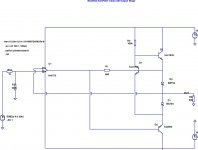
I was thinking of building something similar to the attached schematic.
D382 to D385 would all be the same diode type, see attached FYPF1545DN diode datasheet (they are available from mouser).
Since they are in a plastic package, D383 can be bolted directly to D384, and D382 can be bolted directly to D385. This should provide good thermal bias stability, with no need for mounting any of the diodes on a heatsink or messing about with thermal washers.
Also, since all the diodes are the same type, and because the 4 diamond transistors are of the same type, a reasonably dependable, thermally stable automatic bias current is hopefully guaranteed.
Any comments?
Have a look at my diagram, I think you will need capacitor c4 100nf as shown. Without it I get oscillations. I tried running it with c4 set to 10nf and got oscillation that traveled along the sin wave. The amp ran and never broke out into wild oscillations, but, didn't measure well with c4 at 10nf. The oscillation were subtle, had to zoom in quite a bit to see them. I posted other results in a thread called "a different CAS typology".
Ken
Here is the other thread. http://www.diyaudio.com/forums/solid-state/183144-different-cas-typology-very-low-thd.html
Ken
Ken
Thanks Ken,
Did you experiment with the value of C4 in your schematic above (100nF)? If so, what changes did you observe? Is it present for local loop stability purposes (preventing oscillation) or does it have some other esoteric function?
Also, how does this output stage perform when clipped? Spice suggests it behaves ok with only slight 'sticking' at 20kHz, but how did it fare in the real world.
Thanks for any answers.
Cheers,
Ian
Did you experiment with the value of C4 in your schematic above (100nF)? If so, what changes did you observe? Is it present for local loop stability purposes (preventing oscillation) or does it have some other esoteric function?
Also, how does this output stage perform when clipped? Spice suggests it behaves ok with only slight 'sticking' at 20kHz, but how did it fare in the real world.
Ian,
Got it to work in real life with 100nf and left it alone after that. It's for local loop stability, I'm not knowledgable enough to be esoteric.
Output stage sticks ever so slightly at 20kHz, nothing dramatic at all.
Ken
Time to wake this thread up again - I somehow missed seeing it when it was active.
I was looking for a Class-AB push-pull output stage that could be used either in a fully-discrete opamp, or a hybrid-discrete opamp that uses an existing monolithic opamp, driving a discrete output stage. Here's what I've come up with:
1) I started with Ken Peter's single-ended stage - the one on the right side in the attachment to this post:
http://www.diyaudio.com/forums/soli...r-non-switching-need-revival.html#post2147462
No particular reason for picking on this, except that it was the simplest and therefore the most fundamental.
2) Since there's already voltage swing at the output of the opamp, I eliminated Q1 in Ken Peter's single-ended stage, and fed the opamp output directly to the cathode of the lower schottky. It works, but lacks symmetry and was unsatisfying.
3) Added a PNP (at the previous location of Q1) and drove the base of the PNP from the opamp. Works much better, and is symmetric.
4) Added a resistor from the base to the emitter of the PNP, which biases the opamp's output stage to Class-A.
5) (The key improvement here) Combined this resistor with Ken Peter's R2 into a single resistor, which serves to bias the opamp into Class-A, as well as mop up the residual current from the Schottkys. It simulates with lower distortion, but I don't exactly know why - maybe a feed-forward element is at play.
6) Experimentally replaced the current source I1 with a resistor R1 (probably could bootstrap this for better swings). Distortion is higher, but it's mostly H2, so it's actually better.
Here's a sample LTSpice schematic with the LM6172 and my favourite small-signal transistors - it could certainly be optimized further, but it already looks exceptional. With this output stage, a humble TL071 looks a bit like an OPA627. A high-performance LM6172 looks better than any monolithic available now.
Edit: Thanks, Ken! This one obsoletes my existing discrete opamp (LF01..LF03) output stages, and I'm going to be stuck with an inventory of a few hundred bare PCBs. Serves me right for not spending more time at these forums...
Attachments
Last edited:
I think assessing the circuit on its own, and associated with a high perf opamp can be misleading.
Here is a fairer comparison with a conventional class A PP, and without the help of external loop gain:
I think the figures are telling enough, all the good performances are attributable to the opamp.
In addition, the conventional circuit has a much lower input current, and a higher impedance.
Here is a fairer comparison with a conventional class A PP, and without the help of external loop gain:
I think the figures are telling enough, all the good performances are attributable to the opamp.
In addition, the conventional circuit has a much lower input current, and a higher impedance.
Attachments
I think assessing the circuit on its own, and associated with a high perf opamp can be misleading.
Here is a fairer comparison with a conventional class A PP, and without the help of external loop gain:
...
Fair enough, it looks to be Apples vs. Apples with ~4.8 mA quiescent current for both. I'll take another look, but where mine seems to do better is at lower quiescent currents of the order of 0.5 to 1 mA in the output stage, with higher beta output devices. It also needs to be compared closer to Class B operation, with both transistors coming close to cut off.
Also, 1000uF to bypass the Vbe diode chain in the conventional stage is impractical in most cases. 10uF is a typical value.
Last edited:
R2 is neither a CCS nor a bootstrap,
therefore current in Q1 is variable.
VBE of Q1 not held constant.
Does it matter? I dunno...
You have eliminated Q1 VBE resistor,
that was responsible for bleeding a
constant reserve current that serves
to assure output transistors stay on.
A misbehaving load could turn off a
fast recovering Schottky, but would
be unable to shut off either of the
slow recovering output transistors.
-----
OK I see it now.
The top Q2 (why do you have 2 Q2's?)
conducts R1 to U1 as a reserve current.
The bottom Q2 conducts R2 as a reserve.
Last edited:
R2 is neither a CCS nor a bootstrap,
therefore current in Q1 is variable.
VBE of Q1 not held constant.
Does it matter? I dunno...
I probably should go with a bootstrap or JFET instead of R1. The simulated harmonics became nicer with just a plain R1 - from memory, H2 increased.
You have eliminated Q1 VBE resistor,
that was responsible for bleeding a
constant reserve current that serves
to assure output transistors stay on.
I merged that resistor with another that was intended to bias the driving opamp into Class-A. It works, but maybe the value needs experimenting with.
The top Q2 (why do you have 2 Q2's?)
Sorry, the lower one should be Q3.
I goofed while relabeling the Qs before exporting the schematic (they tend to start with numbers like Q11, Q13, etc. because I sometimes cut them down from some larger circuit like a discrete opamp, and I relabel them left-to-right, top-to-bottom for convenience. LTSpice catches these duplicates, but only if a simulation run is attempted.)
BTW, check out my LF03 discrete opamp schematic at your convenience - I just built the first prototype a couple of days ago, and it does sound good with the present Class-A push-pull output stage.
However, it could potentially give similar performance at lower quiescent current with your non-switching Class-AB stage.
http://www.diyaudio.com/forums/analog-line-level/207871-lf03-discrete-opamp.html#post2928775
I'll post the prototype parts list shortly.
At fisrt glance, the Ben Duncan books looks quite general. Digging into the individual chapters, the big and positive surprise is to realize how precise and accurate Ben Duncan is. The appendixes are unvaluable, plenty of references, plenty of historical info. Many many thanks for pointing this great source of info !
Page 133, about the non-switching amplifiers, it reads :
"This involved a kind of positive feedback, and carrying the risk of blowing-up the output stage ! It also relies on the switching of small diodes, which ameliorated and displaced, rather than overcoming the switching problem".
I guess Ben Duncan didn't wanted to write explicitely that the Technics SynchroBias, marketed as "New Class A", was displacing the problem instead of solving it. The Technics "New Class A" is thus a little bit apart. It should be clear and remembered that JVC "Super-A", Pioneer "Non Switching" and Sansui "Tanaka Non-Switching" are not relying on diodes to be switched.
It is amazing to see the LT1166 biasing integrated circuit, being ignored. Were there commercial power amplifiers using a LT1166 biasing integrated circuit ?
Like Margan, what's worrying me is the behaviour of the output stage when driving a complex load like a loudspeaker. Some optimizations like the ones discussed here may prove unable to cope with capacitive, inductive, or varying impedance loads, especially on non-periodic, non-static, non-symetric input signals like music is. In this context, is there a LTspice standard test gig I can use, for better knowing the behaviour of the output stage ?
Cheers,
Steph
Today I contact LT Technology in this matter because I want to know any Commercial Audio amplifier devices with LT1166 inside.
good luck with that.
it is unusual for device suppliers to say what products are using their specific devices.
mlloyd1
it is unusual for device suppliers to say what products are using their specific devices.
mlloyd1
Today I contact LT Technology in this matter because I want to know any Commercial Audio amplifier devices with LT1166 inside.
Today I contact LT Technology in this matter because I want to know any Commercial Audio amplifier devices with LT1166 inside.
I don't know of any commercial amplifier manufacturer using the LT1166, but I could definitely be wrong. I have always thought it a great part when properly used. Part of the problem is that it is intended for use with MOSFET output stages, and will not work (straightforwardly) with all MOSFETs, due to its need for bias voltage that is a function of gate threshold voltage. Moreover, the designs shown in the datasheet generally are not the best. I show some ways to use the LT1166 in my book.
Cheers,
Bob
hello,
would there be an intellectual property infringement if a company sells three small PCBs, or carrierboards, about 1.5 by 1.0 inch tall, fitted with SMDs, ready to use, providing each one a specific Class AB biaising scheme :
- "New Class A" bias module (see Technics folklore - synchro bias)
- "Super-A" bias module (see JVC folklore)
- "Non Switching" bias module (see Pioneer folklore)
(1) If the technology is published - shows up in a published professional paper.
(2) If the patent has run out of its usual 18 year run.
(Pick one)
Then the the IP is in the public domain according to US law.
The status of IP that is revealed in a service manual seems less clear.
If you can obtain the technical information without signing a NDA, and there is not a currently-running patent, then you are on seemingly solid ground for treating it as if it were in the public domain,.
Big caveat - I'm not a lawyer. When in doubt, ask one.
If there is a violation, then you might get a cease and desist letter which you can honor or not, at your own risk. Until you get the letter...
BTW if there was an issue with infringing IP, simply publishing it on a public forum might get you into all of the trouble you might be in.
Far as I know: The easiest way to assure operation in this class is to cross
deliberately underbiased Schottkys. Thus forcing them to operate upon the
square law curve. You then use this law to re-curve your power transistors
for a super-smooth B crossing! Plus the reserve current always bled by R1.
It doesn't matter that Schottkys operate in Class B and turn off. There is
no significant tail current, and they recover fast. The slow transistors are
always conducting the reserve current, and thus in Class A at all times.
It doesn't matter the exact quiescent current of an underbiased Schottky
B crossing. Its always more than zero, and less than would blow anything.
Will probably drift a bit with temperature. You can bond Q3 Q4 to heatsink
if you want to assure hot drift always floats deeper into B rather than AB...
It probably isn't necessary.
Remember: We are talking about a deliberate underbias. No more than one
half the Schottky stack can ever be fully on at once. We strictly regulate
the voltage sum across the stack, so that could never happen. Runaway
just isn't a likely event, even if you did nothing to thermally compensate.
Whats a Schottky diode gonna dissipate in this application? Less than 2W.
TO-220 packages are common, so thermals are going nowhere! Hot power
devices only do the work, but are never trusted to make the decisions.
The smoothness of the crossing is assured by the quasi-complimentary
square laws, and not by a specific bias current that has to be controlled.
No attempt is made to define what actual small B crossing current might
be? The extra reserve current bleeder assures the power devices will be
operating well above the small crossing of the Schottkys.
I have been reading this post #6 in the first page, it's very interesting. It might be too old and Kenpeter might not even on the forum. I just have a question on this circuit.
From my understanding of the circuit on the left, the voltage drop across R1 is 2Vbe of Q1 and Q2 + 4 schottky diode voltage. The reserve current is through R1. When it swing negative, D1 and D2 are turned off. Q2 is kept on by the reserve current and follow Q1.
If I am right, the reserve current keeps Q1 on all the time, but if D1 and D2 turn off, you still have only Q1 driving the load alone. That is still class B by definition even thought Q2 remains on. How is this having advantage over just the simple ClassAB running into class B when driving low?
Thanks
Last edited:
Member
Joined 2009
Paid Member
There are many non-switching schemes that simply keep both devices conducting but without really contributing to the load and I don't see the point anymore. I used to think it would be a good thing so that cross-over distortion was gone, but you always end up with some other distortion. It seems to me, still naively perhaps, that if you want simple circuits without feedback you need proper Class A and a superb power supply. Otherwise just use Class AB with plenty of feedback and it will have superb performance when designed properly that the case for non-switching AB or full Class A becomes difficult to support. Perhaps one day Class D will reach the point where Class AB no longer makes sense either - at the high end it may be close already but not at the cheap end.
Thanks for the reply Bigun.
I know you were on this thread a lot. Is that the reason this thread got dropped because there is always a catch of something and nobody manage to come up with a design that does not introduce extra distortion?
Maybe that's the reason most schematics of even high end amps don't use this at all and just go on optimizing the crossover distortion and higher loop gain. The only one seems to have success is Pass Lab Aleph current source.
I agree emphatically with all of Bigun's points. I too have noticed that when you manage to reduce the switching issues, you find virtually no improvement in SQ. Whether there is clearly remanent crossover artefacts, OR, as Bigun suggests, the non-switching trick create other distortions, the same result - no improvement to SQ.
Feedback and careful operating points of output devices seems to fix the perceived crossover artefacts. I have found the biggest issues come from the extraction of the fb error, the voltage amplifier, and the drive stage for the output devices. These are the pre-eminent problems; solve them, and a Class AB with some global feedback sounds absolutely ethereal.
Ciao,
Hugh
- Status
- This old topic is closed. If you want to reopen this topic, contact a moderator using the "Report Post" button.
- Home
- Amplifiers
- Solid State
- New Class A, Super-A, Non-Switching : need a revival ?