For safety reason +/-80vdc is maximum suggested voltage, and U can use 4 or 5 pairs outputs.
With +/-67vdc ,and 4 pairs outputs U will have very realable amp.
Regards
Thanks Miles.
")
IRFP240 | IRFP9240
Hi
I see these components used together often, but I can't understand why one would use N-ch and P-ch transistors as complements that are as significantly different from each other as these are? Gm is really one of the most important parameters to regard here. IRFP240 has 11 S of transconductance. IRFP9240 is only half that at 5.7 S. IMHO, and my experiences with employing verical fets as linear output devices, matching Gm is more important than input capacitance or even breakdown voltage. Not being able to set the bias to be optimum for both devices (the optimum bias level is related to Gm) you will pay for it at the current crossover in the form of extra distortion. It is impossible to use two significantly unequal Gm devices and set an optimum bias for both. If it were me, I would complement the IRF240 with one such as SFH9154 or similar. So what if the package isn't even exactly the same? Matching CISS or Vds will usually never yield two complements of equality in the realm of switching type vertical power fets.
Yeah, unfortunately availability does have an effect on the devices you choose.
If larger source resistors are used for the N-ch than for P-type, the mismatch in Gm may be reduced a bit. Bob Cordell mentioned once of using different values of source resistors for differing Gm components achieving better 'matching'.
If larger source resistors are used for the N-ch than for P-type, the mismatch in Gm may be reduced a bit. Bob Cordell mentioned once of using different values of source resistors for differing Gm components achieving better 'matching'.
If larger source resistors are used for the N-ch than for P-type, the mismatch in Gm may be reduced a bit. Bob Cordell mentioned once of using different values of source resistors for differing Gm components achieving better 'matching'.
I think the different gm is a red herring.
The feedback makes the output correct.
It isnt the gm of the MOSFETs that makes the output correct, its the LTP and VAS.
So matching transcoductance curves is not important to crossover and achieving a smoother transistion into class B region?
 (for the n'th time... )
Relying on a fb loop to fix the extra crossover distortion and all the other non-linearities is like placing a dry bandage on top of a puss oozing infected sore. FB may shift freq of distortions to higher orders since the two input signals, the input source and the GFB, arrive to the input stage at different times due to phase shifts in the amplifier. This may be better or worse depending how FB is employed and what is whithin the loop. There is no substitute for striving to design each amplifier stage, with or without local loops, individually to be as linear as possible to the global loop. In an ideal world GFB corrects everything, and amplifiers have no phase margin, but the real world is not ideal. Real transistors suffer from propagation delay. If you have a stage that produces larger higher order components to start with, such as with crossover from a comp source follower using 'mis-matched' vertical fets and all of thier non-linear capacitances, you can use a local FB scheme making the stage appear less corrupt to the global loop. A bit of the pay off is lower distortion and higher BW.
(for the n'th time... )Relying on a fb loop to fix the extra crossover distortion and all the other non-linearities is like placing a dry bandage on top of a puss oozing infected sore. FB may shift freq of distortions to higher orders since the two input signals, the input source and the GFB, arrive to the input stage at different times due to phase shifts in the amplifier. This may be better or worse depending how FB is employed and what is whithin the loop. There is no substitute for striving to design each amplifier stage, with or without local loops, individually to be as linear as possible to the global loop. In an ideal world GFB corrects everything, and amplifiers have no phase margin, but the real world is not ideal. Real transistors suffer from propagation delay. If you have a stage that produces larger higher order components to start with, such as with crossover from a comp source follower using 'mis-matched' vertical fets and all of thier non-linear capacitances, you can use a local FB scheme making the stage appear less corrupt to the global loop. A bit of the pay off is lower distortion and higher BW.
So matching transcoductance curves is not important to crossover and achieving a smoother transistion into class B region?
)
Yes basically.
Feedback forces the output transistor to amplify linearly even if the output transistor is grossly unlinear.
I use IRFP240/9240 for about 7 of my designs and they are switching transistors yet I get excellent results.
Feedback forces the output transistor to amplify linearly even if the output transistor is grossly unlinear.
If you say so. I will forget about all the research about FB theory that proves otherwise.

Logically speaking, for every distortion created and fed back, the input stage must create an anti-distortion signal to the output, which is then amplified by the VAS and drivers. Crossover distortion creates very high frequency components because of the steep slope of the output signal related to it. It is well worth the effort to keep this distortion as small as possible at the output stage. (This also means with vertical fets a bias of couple hundred mA to prevent the load line from venturing into the 'transconductance drop zone' as I call it, the area close to cutoff where Gm drops significantly wrt Id. see below) The high frequency garbage related to crossover is well above the BW limit of the global loop and are not canceled. The BW is limited by propagation delay and phase margin of the global loop, delay between the FB signal and the input reference. Using local loops can create a more linear system presented to the global loop requiring less compensation and increasing the overall frequency that the amp can amplify and still be unconditionally stable.
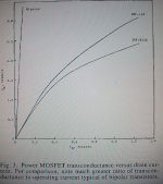
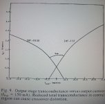
1st graph shows Gm vs Id(c) comparison of FET to BJT. Notice the constant steep slope of the line for BJT. 2nd is class AB and crossover area of Gm vs Id. As you can see, biasing FETs as if they are BJT's with 25mA or so will leave a 'hole' in transconductance through the current crossover operating region resulting in crossover distortion.
[graph ref. Mr Cordell's EC mosfet paper.]
Attachments
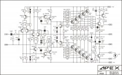
Q9 and Q10 run with 30mA, bias of the output tranzistor 200mA set by P1, and bias stay stabil. Maybie must corect after few minutes but that will be small corection.
I must repeat, outputs not run with 25mA or 30mA, it's biased with 100mA (200mA with large heatsinks) per mosfet. VAS transistors current is 30mA and it's must be on main heatsink with outputs.
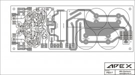
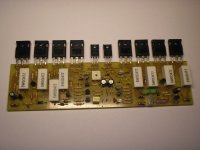
PSU for DIY with soft-start and DC protect. Transformer 1kVA sec: 2x55V 8A + 24V 1A.
PCB size: 200x75mm
Hi Mile,
where did you post the schematic of the PSU-7?
also, what's the difference between your HV23 and HV350?
seems shematics are the same...
Thanks in advanced.
Joel
Hi Mile,
where did you post the schematic of the PSU-7?
also, what's the difference between your HV23 and HV350?
seems shematics are the same...
Thanks in advanced.
Joel
There is no schematic for PSU-7 only pcb layout.
Difference between HV23 and HV350 is only in BIAS circuit.
Regards
Thanks for the info.
Regards.
You can draw schematic from pcb layout, it's simple circuit.
Regards
Attachments
My immediate thought here is that clearance between the low voltage and line voltage parts needs to be increased substantially - there should be 10-15mm at least
Low voltage is from protect separate psu, and there is gnd track around them.
hi apex kindly send me the pcb desin for #27 thanks
I started too many threads already, and this amp will be for share in future.
Regards
- Home
- Amplifiers
- Solid State
- MOSFET Amplifier IRFP240/IRFP9240