The relevant capacitance is the gate-drain capacitance C_gd. The datasheet sais C_gd < 300pF @ V_gs>10V (and almost disappears for higher V_gs) and C_gd_max=1250pF (@0V V_gs)
there's an error, it's supposed to say:
C_gd < 300pF @ V_ds>10V (and almost disappears for higher V_ds) and C_gd_max=1250pF (@0V V_ds)
Very interesting consideration. I partially agree with you.According to the datasheet the C_gs of an IRFP240 is max 1.2nF. But the V_gs is only changing about 0.5V while the output swings 75V. So the effective C_gs presented to the VAS is about 0.5/75*1n2=8pF and can therefore be neglected.
One can see the circuit from the devil's advocate, worst case analysis.
Consider that the load (the loudspeaker) is 4 Ohm. This is a very small impedance compared to what we expect in the collector of the VAS.
I don't say here that it shows on the collector of the VAS.
But you will agree with me that the VAS gets a path to it (to the load) through the C_gs capacitance. Which is 1200pF maybe as you wrote.
So now, look what's happening when you need to swing a large voltage on the load, which means a large output current. You'll need to go from a Vgs voltage equal to maybe 2V (the MOS was OFF), to a Vgs maybe equal to 4V (the MOS conducts some current). When the MOS conducts, the current flows in the load, and the voltage greatly increase, maybe a 40V swing. We thus need an increase of 2V on Vgs, which then (automatically ?) commands a 40V swing on the load.
A voltage of 40V on the load means 10 Amp in a 4 Ohm load.
A 10 Amp in the load, commanded by a Vgs increase of 2 V, makes an overall transconductance equal to 5 Siemens.
I think we are okay with these parameters. The orders of magnitude seem correct.
With the above example, can we thus conclude that seen from the VAS collector, the parasitic capacitance is not equal to 1200pF, but equal to 1200pF divided by 20, which is the ratio between the Vout swing (40V) and Vgs swing (2V) ?
If this is a valid devil's advocate, worst case analysis, is is valid to say that the effective C_gs presented to the VAS is about 1200pF/20 = 60pF ?
Instead of the 8pF you have quoted.
I wrote "We thus need an increase of 2V on Vgs, which then (automatically ?) commands a 40V swing on the load."
If there is any glitch about the idea of "automatic", then we face the plain and ugly situation of the VAS stage seeing a 1200pF parasitic capacitance, not connected to ground, but connected to the 4 Ohm load, which for the VAS point of view is a ground, roughly.
Are there mechanisms making the above process less than "automatic" ?
MOSFETs are not infinitely fast.
However, with their 50ns turn-on time, rise time, turn-off time, we may assume they are infinitely fast for audio frequencies.
1. From the devil's advocate, worst case analysis, are there delays or other effects to be taken into account, in the µs range, that cannot be neglected for audio applications ?
2. Don't you think that the 5 Siemens transconductance that we have taken into consideration, may be much lower when the amplifier is operating at low power (below 250 mW - home HiFi use), setup with a low bias current (maybe 25 mA in each MOS) ? The transconductance may be 3 times smaller, hence the effective C_gs presented to the VAS to be multiplied by 3, making it equal to 60pF * 3 = 180pF. Per MOSFET !
Any comment welcome.
Very interesting discussion.
Attachments
Thats the thing with the human mind. We tend to simplify things down to an almost absurd level so we can get a glimpse of understanding (just as I did before), but then we already might have overlooked some important things, or our simplified modell no longer applies to the real world.So now, look what's happening when you need to swing a large voltage on the load, which means a large output current. You'll need to go from a Vgs voltage equal to maybe 2V (the MOS was OFF), to a Vgs maybe equal to 4V (the MOS conducts some current). When the MOS conducts, the current flows in the load, and the voltage greatly increase, maybe a 40V swing. We thus need an increase of 2V on Vgs, which then (automatically ?) commands a 40V swing on the load.
We also tend to tweak the assumptions that go into our simplified model (the devil's advocat) so that we get the result we expect. (Just as I did before)
At the end of the day one "can" calculate the amount of the capacitance C_gs that contributes to the capacitance presented to the VAS asIf this is a valid devil's advocate, worst case analysis, is is valid to say that the effective C_gs presented to the VAS is about 1200pF/20 = 60pF ?
Instead of the 8pF you have quoted.
C_p(V_out) = C_gs(V_ds)/(g_m(I_d)*R_Load). (One can get the idea.)
Note all the dependancies, that cannot be neglected.
But I would only rely on an actual measurement, or maybe on a spice simulation, if properly conducted.
You forget to mention the gm of the FETs that is also connected to the load and C_gs. I'm sure you had it in mind.If there is any glitch about the idea of "automatic", then we face the plain and ugly situation of the VAS stage seeing a 1200pF parasitic capacitance, not connected to ground, but connected to the 4 Ohm load, which for the VAS point of view is a ground, roughly.
It's maybe like saying, its hard to press the gas pedal as I (the VAS) will have to move the whole car, but forgetting that theres an engine (g_m) under the hood helping me with that.
I know that is not what you are saying, but i found the image quite interesting to stress the importance of the g_m.
PS:
And actually this whole discussion is one of the reasons (maybe there are more, I don't know yet) I will use an emitter follower driver stage before my FETs
")
Last edited:
I still dont see anything special about the cfp vas, has been used for a very long time, I have them in amps I built 15 years ago, theres nothing unique about it, works well because it has high input impedance.
Ideally those mosfets should be driven by a emmiter follower for good performance, even better use them in a triple configuration.
Krachkista if you go through Bob Cordells thread BJT vs Mosfet I think it was youll find many more reasons to use a emmiter follower than just the parasitic capacitances.
Steph tfs, I find it amusing you say that those bc parts are better than the toshiba parts, you obviously havent done a thorough analysis like you did with the rest of the amp. The toshibas have far less noise (think of the effect of rbb, especially when using large degeneration) and the beta easily match or better those of the bc parts, their Vce is more than adequite for the voltages of this circuit. Also theres other factors to consider, once again capacitances, early voltage ......
As experience audio designer to explain to audience why this schematic amplifier is not good, is not very simple.
The practical explanation is sometimes simplest: Try to put this amplifier with output mosfet IRF240/IRFP9240 in clipping (high input signal) but without load (loudspeakers).
The amplifier will burn. Before you do that have on mind that I already do that in the past. The only Mosfet at output stage which will not burn is form 2SK/2SJ audio series but if you look their characteristic carefully they have more common with transistors then with POWER MOSFETS.
The conclusion form respect Mr. T.Leach that mosfet is not suitable for output audio stages are true.
The amplifier will not burn at clipping level without load.As experience audio designer to explain to audience why this schematic amplifier is not good, is not very simple.
The practical explanation is sometimes simplest: Try to put this amplifier with output mosfet IRF240/IRFP9240 in clipping (high input signal) but without load (loudspeakers).
The amplifier will burn. Before you do that have on mind that I already do that in the past. The only Mosfet at output stage which will not burn is form 2SK/2SJ audio series but if you look their characteristic carefully they have more common with transistors then with POWER MOSFETS.
The conclusion form respect Mr. T.Leach that mosfet is not suitable for output audio stages are true.
At the end of the day one "can" calculate the amount of the capacitance C_gs that contributes to the capacitance presented to the VAS as
C_p(V_out) = C_gs(V_ds)/(g_m(I_d)*R_Load). (One can get the idea.)
Note all the dependancies, that cannot be neglected.
But I would only rely on an actual measurement, or maybe on a spice simulation, if properly conducted.
I agree on the formula !
Where can I find a vertical power MOSFET spice model, providing decent accuracy regarding the g_m dependency in function of I_d ?
Good hint Homemodder. Thank you.
http://www.diyaudio.com/forums/solid-state/101745-bob-cordell-interview-bjt-vs-mosfet-3.html
@ steph_tsf
take a look at post 24.
On the IRF page you can download subcircuit models of their FETs.
I don't to how detailed or accurate they are though.
http://www.diyaudio.com/forums/solid-state/101745-bob-cordell-interview-bjt-vs-mosfet-3.html
@ steph_tsf
take a look at post 24.
On the IRF page you can download subcircuit models of their FETs.
I don't to how detailed or accurate they are though.
I agree on the formula !
Where can I find a vertical power MOSFET spice model, providing decent accuracy regarding the g_m dependency in function of I_d ?
.subckt IRF640 D G S
.model mosfet NMOS( LEVEL=17 VTO=3.869 RS=0.01909 KP=7.151 RD=0.0981 TC1RD=0.0126 RG=6 IS=1e-36 LIMIT(VDS)=(*, 200)
+ CGDMAX=4.00E-09 CGDMIN=1.00E-11 XG2CGD=0.5 XG1CGD=0.1 CBD=3.38E-10 VTCGD=0.8)
.model diode D( IS=2.10e-12 RS=0.0125 TT=4.673e-07)
M1 D G S S mosfet
D1 S D Diode
Cgs G S 1.19E-09
.ends
.subckt IRF9640 D G S
.model mosfet PMOS( LEVEL=17 VTO=-3.608 RS=0.0724 KP=8.645 RD=0.3095 TC1RD=0.0128 RG=13.171 IS=1e-36 LIMIT(VDS)=(-200,*)
+ CGDMAX=2.30E-09 CGDMIN=2.00E-11 XG2CGD=0.3 XG1CGD=0.1 CBD=3.34E-10 VTCGD=2)
.model diode D( IS=1.17e-28 RS=0.0634 TT=4.617e-07)
M1 D G S S mosfet
D1 D S Diode
Cgs G S 1.07E-09
.ends
If you had used Lateral Mosfets in the output stage then i guess you could get away with such a simple biasing scheme. Lateral Mosfets have a negative temperature coefficient so they'll tend to reduce quiescent current as they heat up.
IRFP240 & it's complement have a positive temp coefficient (until they are drawing many Amps of current) so they'll conduct more current as they heat up. There is no allowance for this in your circuit diagram, you'd need something similar to what is used in a transistorised output stage.
I might be wrong, but i don't think so
A negative temperature coefficient (NTC) occurs when the thermal conductivity of a material rises with increasing temperature
A positive temperature coefficient (PTC) refers to materials that experience an increase in electrical resistance when their temperature is raised.
so I see no problem.......
Try glueing the bias transistor to an output transistor and that works well.
Sometimes too well !
I run my amps with a household iron on the heatsink to test it upto 100 degrees for thermal runaway. As yet had no problems with IRFP240/9240.
I do tend to run a minimal bias tho. Less than 10mA seems to get rid of crossover distortion.
Nigel, does that mean you running those mosfets without a vbe multiplier too???
I use a simple Vbe multiplier but one not mounted on the MOSFETs or heatsink.
OK I was just checking if you were getting away without it, the only way I use these mosfets and I dislike using the IRF parts as the toshibas ae so much better is in triple configuration. This way I get away using a small signal transistor glued to the heatsink or the mosfet itself. I run 100ma bias through them, I really cant understand how you can get away with 10ma bias although Ive never tried either, I guess some more experimenting is needed.
OK I was just checking if you were getting away without it, the only way I use these mosfets and I dislike using the IRF parts as the toshibas ae so much better is in triple configuration. This way I get away using a small signal transistor glued to the heatsink or the mosfet itself. I run 100ma bias through them, I really cant understand how you can get away with 10ma bias although Ive never tried either, I guess some more experimenting is needed.
I apply a 1 volt sine wave to the input, connect a speaker then slowly wind up the bias current until crossover distortion goes. The crossover distortion is really bad to start with but quickly goes around the 10mA mark.
The 10mA or less I usually get is for one pair of output transistors.
I found a good way of testing bias circuits was to heat up the heatsink with a household iron upto about 100 degrees and look for thermal runaway while monitoring the bias current.
How is overall distortion figures say into 20Khz.
This is the configuration I use with V mosfets, anything else just doesnt sound good to me. Without proper drive these V mosfets seem to have a lack of low down bass compaired to BJTS.
Attachments
How is overall distortion figures say into 20Khz.
This is the configuration I use with V mosfets, anything else just doesnt sound good to me. Without proper drive these V mosfets seem to have a lack of low down bass compaired to BJTS.
It looks OK on the scope.
It sounds fine too which is the deciding factor for me.
The conclusion form respect Mr. T.Leach that mosfet is not suitable for output audio stages are true.


Whatever
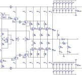
I just ran a couple of Spice simulations using Tina 7 Texas Instruments. The result came as a surprise to me. It is possible to get a fast amp and still delivering low THD using a cascoded J-FET input stage biased at 1.25 mA in each FET, feeding a cascoded VAS biased at 25 mA without a complementary Darlington arrangement (thus, no more a Sziklai pair) and without emitter followers.But I would only rely on an actual measurement, or maybe on a spice simulation, if properly conducted.
So, using a simple circuit, we get a 700 KHz -3dB corner frequency and a slew-rate (dV/dt) of about 150 V/µs.
So yes, like krachkiste wrote, it definitely proves that the effective C_gs seen by the VAS is heavily divided by the Gm (combined to R_load) provided by the MOSFET. C_gs gets divided by something like between 20 to 100, depending on the load.
Moreover, putting MOSFETs in parallel doesn't impact dV/dt. On one side, you multiply the C_gs capacitance, but on the other side, you also multiply the Gm factor.
Attached you will find a schematic for such fast & low THD amp, edited under Tina 7 Texas Instruments, ready for simulation.
Please note the VAS emitter decoupling network.
You can download Tina 7 Texas Instruments free of charge here SPICE-Based Analog Simulation Program - TINA-TI - TI Tool Folder
Just one thin doubt : the MOSFET simulation model doesn't take into account possible dependencies of C_gs in function of I_d. It means that the simulation is maybe valid regarding dV/dt, but less valid regarding THD.
And actually this whole discussion is one of the reasons (maybe there are more, I don't know yet) I will use an emitter follower driver stage before my FETs
According to this simulation, the last thing to do would be to add an emitter follower stage between the VAS and the MOSFETs. Can you explain again why you want to add an emitter follower stage ?
Attachments
Last edited:
- Home
- Amplifiers
- Solid State
- MOSFET Amplifier IRFP240/IRFP9240