This design can not be modified to use only N-tip mosfet. I have quasy-complementary design with IRFP250 and I post to you.Dear mr. Apex (sorry this is th name i could find) , Thanks for a nice design. question is can it be modified only with IRFP250 on both side . I would we gratefull to get a design with those hexfet,s thanking Vedmitraa
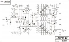
Why anyone have no any coment on unusuall circuit Q8,Q9,R17,R21 and Q7,Q10,R18,R22 in voltage amp...
It is not that much "unusuall" and it certainly isn't new.
http://www.diyaudio.com/forums/solid-state/88515-cfp-vas.html
I've been using CFP VAS in my "Studio" amplifier since 1975-76.
hi apexaudio,
this is a very interesting circuit you are bringin in ! Thanks !
At first glance one may think that the slew-rate is going to be low, and that thermal stability will be poor. But looking again to the schematic, one discovers Q9 and Q10, quite unusual indeed.
No doubt you like energic local feedback ! With Q1 and Q2 passing about 1.5 mA each, a 100 Ohm emitter resistor is something important compared to the equivalent internal emitter dynamic resistance of approx 17 Ohm. Many will consider this as a waste, and will advise using 18 Ohm for Q1 and Q2 emitter resistors.
Which means that you don't like high open loop designs.
You prefear moderate open loop designs, with a kind of dynamic range extension at the input.
And 1.5 mA bias current in each long tailed pair transistor, at the input, is something solid, three times more than the usual 0.5mA value.
Hope you have the same beta for the NPN and the PNP long tailed pairs, otherwise you'll easily get unacceptable DC offset at the output.
Have you considered using a DC-servo arrangement, with an integrating op-amp (OPA-134 or OPA-2134) automatically zeroing the DC offset at the output ? This will allow you to shortcut C3 and C4, I'm sure you don't feel comfortable with them ...
But remember : if you use DC-Servo, then the integrator capacitor(s) are to be considered as in the audio path. Don't use cheap integrator capacitors, and pay attebntion the way you mount it (them).
Let us now see the Vas stage.
R10 develops 1.5 mA x 2K2 = 3.3V.
This is a quite high voltage compared to mainstream designs.
It helps stabilize the Vas quiscent current. There won't be any issues on that aspect.
Then most people get a problem.
It is not so easy to determine the Vas quiescient current because of the presence of Q9 (and Q10).
Let us ignore Q9 (and Q10), as a starting point.
R21 may thus see a voltage of 3.3V less 0.65V (Q8 Vbe) = 2.65V.
Which means 26.6 mA in R21 (100 Ohm).
That's quite a solid quiscient current for a Vas stage.
Good !
But wait a moment, this current is not entirely drawn by Q8, as we have Q9 close to him.
One way to look at the circuit is straightforward : we know that Q8 + Q9 current equals 26.6 mA because of R21.
The only remaining question is how they share this value.
Well, with R17 equal to 1K, one may thus say that Q8 contribution is quite small, and equal to .65/1K = 0.65 mA.
This is quite interesting : the Q8 Q9 compount makes Q8 working as little as possible, with 1.6 mA, preserving linearity and bandwith, and it is Q9 that effectively boosts Q8 work, sinking about 26 mA quiescient, and ready to modulate that current for driving the quad vertical MOSFETs that follow.
But Q9 is no brute force like a plain and trivial emitter follower ! One must remember that any milliamp Q8 draws, causes a drops on Q8 emitter voltage (thanks to R21), hence a neat local negative feedback.
Excellent !
The more I'm looking to this circuit, the more I love it !
Audio freaks may love this kind of energic local feedback alot !
But one shoud expect a poor THD performance.
Because of high local feedback, generating a moderate open-loop gain.
But wait a moment. Does this circuit have a chance, being adopted by audiophile freaks ? Let us think like they think. Due to the fact the the circuit is beautifull, fully symetric, the H2 harmonics won't show. And it should be remembered that audio freaks love amplifiers delivering the same amount of H2 and H4 harmonics, than H3 and H5 harmonics. You only can reach this with asymetric circuits like a single-ended triode, or a very old fashioned semiconductor output stage like in the NAD3020 amp, using a quasi-complementary pair relying on antique 2N3055 NPN bipolar power transistors.
Let us now see how the Vas stage does saturate, like needing to push a lot of current into the 800 pF x 4 = 3200 pF MOSFETs gate capacitances.
The Vas stage gets driven by the long tailed pair.
If the long-tailer pair saturates, Q4 will sink about 3mA (twice the quiescient current). It generates 6.6V on R10 (2K2). This translates to 5.35V on R21 (100R), hence a Vas current of 53mA.
More Vas current than 53mA cannot be expected.
A current of 53mA in 3200 pF defines a slew-rate of 16V/µs.
That's too slow by modern standards !
And maybe we should count 6400 pF instead of 3200pF as load (the other 4 MOSFETs are there), so the slew-rate may be completely inadequate, with only 8V/µs.
That's quite worrying.
This needs to be corrected / improved.
But okay, I see the advantage of the Q8 Q9 compound : Q8 doesn't get stressed by the 53mA delivery, as it nearly works with a constant current of 0.65mA. That's very good for the interstage linearity. Q8 doesn't materialize a fancy load for the long tailed pair.
Waow ! Looks like a genius sketched this circuit. But he got caught by the dV/dt.
I won't argue about potential thermal runaway. To me, yes, without further investigation, my first appreciation is that this circuit may suffer from thermal runaway. The use of a variable resitance (P1, R19, R21) as bias controlling element is "verboten" when using vertical power MOSFETs. Many people will tell you that your design may be okay if you are using vertical power MOSFETs, like modern equivalents of Hitachi 2SK/2SJ series.
Don't you think it is possible to split C6 and C7 into two high-frequency compensation schemes ? C6 and C7 at 100 pF each is too much in a Vas stage ! Those Miller capacitances may indeed help get a good stability, but they will ruin the gain-bandwidth product. And possibly, also ruin the dV/dt. A value like 100pF for C6 and C7 looks very bad indeed, like there is a dog in the circuit at high frequency.
But don't you think that C6 and C7 at 22 pF each can be okay, and in case of instalility, putting one compensation capacitor between Q7 base and the output (maybe 68 pF), and also one compensation capacitor between Q8 base and the output (maybe 68 pF also) ?
When doing what's stated above, C5 may get it's value lowered, from 22pF to 4.7pF maybe.
I would suggest that you test a new circuit, bringing your ideas more forefront :
- only use one pair of MOSFETs at the output. This way the capacitive load on the Vas stage is only 800 pF per MOS (possibly 1600 pF if you count the other half)
- go for lateral MOSFETs instead of vertical MOSFETs. Good lateral MOSFETs are ALF08N16V (N-channel) and ALF08P16V (P-channel) from MAGNATEC, 160V 8A TO-247, source connected to case. They need low bias voltage, like former Hitachi 2SK/2Sj series. They are inherently stable regarding their bias current, so it may not be needed to use a thermally-coupled Vbe multiplier as bias controller. Your resistor arrangement may suffice.
- double the Vas quiesecent current, up to 50mA. This way you will be able to drive 100mA max in 1600pF for a decent 62V/µs slew-rate. That's the bare minimum, but if on the other hand your circuit delivers smooth & wide audio, it will be loved by many.
- add a cascode stage on the Vas. Avoid Q8 experiencing the full voltage swing. Put an inbetween-transistor somewhere between Q8 and Q9, that will endure the voltage swing, and still biased as a low 0.65mA like Q8 is. This way you may split all the constraints, for an improved linearity. Q8 working at constant Ic and low Vce like 5V, Qx (the inbetween new guy called cascode) working at low Ic (nearly like Q8) and enduring the voltage swing, and finally, Q9 enduring the 26mA quiescient current (and 2 Watt dissipation under 75V).
- if you are not allergic to cascode circuits, why not trying a cascode arrangement on the differential pairs ? A voltage like nearly 75V on the collectors of the input pairs make me scary. I don't trust low voltage low noise semiconductors beyond 42V. Are you sure Q2-Q2 (2SA970) and Q4-Q5 (2SC2240) are reliable in such context ? If you have a thin doubt, and if you feel they get unobtainable or expensive, the best is to evolve to a cascode arrangement. Same strategy as above with the Vas : you let the differential pair operate at a moderate collector voltage like 5V (excellent noise specs), and you add an "inbetween pair" called cascode, to endure the static voltage, about 67 Volt. Then you can substitute the 2SA970 and the 2SC2240 transistors in favour of more moden stuff, wishtanding less voltage (about 35V maybe), but offering more current gain, less noise, and significantly less expensive, and possibly sorted by current gain at the factory. Have a look to BC549C and BC559C transistors.
- a poor's man solution regarding the above point would be to forget about the cascode arrangement, and to insert 47V zener diodes in Q1-Q2 and Q4-Q5 collectors.
Some will prefear returning Q5 (and Q2) collector to the emitter of Q8 (and Q7), straigt, without R11 (or R7). This marginally increases gain. And may simplify PCB design.
Some may want increasing the AC open loop gain by bypassing R21 (and R22) by a capacitor of 1000µF/16V plus 22 Ohm in series.
This way THD may be divided by 4 from 20Hz to 20Khz.
That's all I can say for the moment.
Thanks for sharing this very interesting circuit.
Hope you will suceed designing a Vas cascode, still retaining the advantage of this design, which indeed is not a dumb emitter follower pre-driver.
This circuit definitely needs consideration, and let us hope you will be able to bring it to next stage.
Cheers !
Last edited:
That's all I can say for the moment.
Cheers !
Thanks for the few!!
Indeed, a complete coverage with competent explanations.
Good work, steph.
sorry, I made a typo
please read :
" To me, yes, without further investigation, my first appreciation is that this circuit may suffer from thermal runaway. The use of a variable resitance (P1, R19, R21) as bias controlling element is "verboten" when using vertical power MOSFETs. Many people will tell you that your design may be okay if you are using lateral power MOSFETs, like modern equivalents of Hitachi 2SK/2SJ series."
And sorry for the attached file, it is not there because of exceeding the max .pdf size on this forum.
Try this link maybe : Magnatec. ALFET Lateral MOSFETs
You may then download the Audio Catalogue (right side on the webpage).
Last edited:
sorry, I made a typo
please read :
" To me, yes, without further investigation, my first appreciation is that this circuit may suffer from thermal runaway.You may then download the Audio C
With my IRFP240/9240 amps I tend to run as low a bias as possible, just enough to kill crossover distortion. A new one I built tonightwith single output pair is running on a bias current of 7mA and sounds great at all volumes.
i don't recall the spec for the input capacitance for these particular mosfets, but i think the effective input capacitance is significantly reduced (i.e. less than 800pF per device) by the local negative feedback courtesy of the source follower configuration.
")
mlloyd1
mlloyd1
hi apexaudio,
... like needing to push a lot of current into the 800 pF x 4 = 3200 pF MOSFETs gate capacitances ...
i don't recall the spec for the input capacitance for these particular mosfets, but i think the effective input capacitance is significantly reduced (i.e. less than 800pF per device) by the local negative feedback courtesy of the source follower configuration.
mlloyd1
Right on , mlloyd, they are more or less neutralized by the
source follower scheme, as it s a bootstrap, which in that
case is local POSITIVE feedback...
Thanks Steph,
Your post is a reson to share this circuit. I agree with your sugestion, but this is discounted prodact for DIY. This is next step for beginers after building Gainclones. Sorry I dont speak English, I hope you understand me?
Best Regards for all Diyers, make amplifiers for fun not for competition.
Your post is a reson to share this circuit. I agree with your sugestion, but this is discounted prodact for DIY. This is next step for beginers after building Gainclones. Sorry I dont speak English, I hope you understand me?
Best Regards for all Diyers, make amplifiers for fun not for competition.
i don't recall the spec for the input capacitance for these particular mosfets, but i think the effective input capacitance is significantly reduced (i.e. less than 800pF per device) by the local negative feedback courtesy of the source follower configuration.
mlloyd1
But you aren't just driving "capacitance", the moving target...
You ARE driving Qg/Gm. Any change in channel current can
only come because of a change in gate to channel charge.
This change takes energy, even if you fudge away Farads.
Dear Steph_tsf, thanks for sending us webpage of new ALFET MOSFETs. I'm visiting this page for the first time. My impression regerding difference toward 2SK/2SJ audio series is not so great.
The Mosfet have only higher dissipation. The all other characteristics are the same.
The Mosfet have only higher dissipation. The all other characteristics are the same.
A cap between emitter of Q9 and emitter of Q10 provides AC coupling between the OPT gates and allows the negative driver to discharge the positive mosfet gates and vice versa.
It appears to me that Q11 and Q12 already perform this function?
Multiplying the gate capacitance of Q13 and Q17 to span the gap
between the driving Sziklai pairs. Perhaps even Gm of the MOSFET
source contributes to the gain of this capacitive multiplier? I would
expect this span voltage to actively hold a very stable threshold.
Then again, does cap multiplier also make the gate harder to drive
by exact same amount? I havn't really done the math on this one.
Probably depends wether gate threshold or capacitiance dominates
control of Q11/12? I think I've gone and confused myself now.
And then to digest that in context that MOSFET gate cares only
Coulombs in/out, any value of "capacitance" depends upon the
circuit. I'm beyond lost now, and not really helping the situation...
Last edited:
Q11 and Q12 are for limiting the output current, and are supposed to have no effect during normal operation at all.
According to the datasheet the C_gs of an IRFP240 is max 1.2nF.
But the V_gs is only changing about 0.5V while the output swings 75V. So the effective C_gs presented to the VAS is about 0.5/75*1n2=8pF and can therefore be neglected.
The relevant capacitance is the gate-drain capacitance C_gd. The datasheet sais C_gd < 300pF @ V_gs>10V (and almost disappears for higher V_gs) and C_gd_max=1250pF (@0V V_gs)
So it very much depends on the output voltage, wether the FET-capacitances are a limiting factor or not. But most of the time they should not be.
- Home
- Amplifiers
- Solid State
- MOSFET Amplifier IRFP240/IRFP9240