Hi to all,
I want to start that project but I am little confused: vhat tis better solution, HV350.2 or HV23? What is differents?
Thanks in advanced.
HV23 from post #470
http://www.diyaudio.com/forums/solid-state/162043-mosfet-amplifier-irfp240-irfp9240-47.html
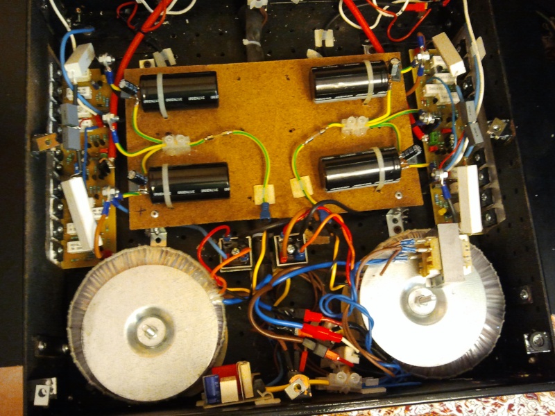
it is really strange ..........., the strangest thing that the problem is the same for the two PSU, so it should not be a broblema capacitors. Last attempt, I disconnect the output RC filter (1 Ohm/17W in series with 680nF) .... let's see what happens?
.... solved, the problem was the capacitors have replaced them with 4 new from 10000uf 100v
This is what I use. The 100pF on the BC557B prevents oscillation. Without that the circuit oscillates . Not sure if it is optimum . Haven't had time to investigate that yet.
Hello,
this type of preamp / circuit, as a measure output impedance, input impedance? bandwidth ?
thanks
Hello,
this type of preamp / circuit, as a measure output impedance, input impedance? bandwidth ?
thanks
sorry ... another question; R2 is 10 ohms? input does not include a capacitor? output is 1uF electrolytic?
sorry for all these questions ...
hi for all !
A question, whats the maximum voltage I can put in the amplifier ???
86+86v is safe ?
Only with 8R load.
 ?
?Hi apexaudio!
What pre-amp would you recommend for this amplifier? Maybe with schematic+PCB already posted by you on diyAudio?")
Hello, add me to the same question!
FET Buffer Preamp
#374 - http://www.diyaudio.com/forums/solid-state/162043-mosfet-amplifier-irfp240-irfp9240-38.html
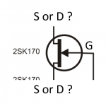
How do I know which leg is drain and which is source on the FET devices? It seems the same - and I cant know for sure if you mirrored some of them.
All vertical mosFETs have Drain in the middle.
Source is on the right and gate is on the left, GDS
All Lateral mosFETs have Source in the middle, GSD
That's with the tab pointing UP, and the markings toward you.
All vertical mosFETs have Drain in the middle.
Source is on the right and gate is on the left, GDS
All Lateral mosFETs have Source in the middle, GSD
That's with the tab pointing UP, and the markings toward you.
Thanks, but I am aware of the physical layout of the transistors - I was talking about the logical layout in the schematic - sorry if I was'nt clear.
It takes 20 secs to find a reference on the net. Just posting a link is surely quicker than discussing what is out there. https://learn.sparkfun.com/tutorials/how-to-read-a-schematic/schematic-symbols-part-2
FET Buffer Preamp
Hi Apex, do you have PCB for this pre-amp ?
Thank you !
It takes 20 secs to find a reference on the net. Just posting a link is surely quicker than discussing what is out there. https://learn.sparkfun.com/tutorials/how-to-read-a-schematic/schematic-symbols-part-2
Thanks Ian, but if you look at the schematic posted by apex (link in my first post), you see that both n and p-channel fets legs D & S are the same - you cant tell the difference - that is what is getting me confused. Please look at my attached picture.
The link you posted shows different kinds of p/n mosfets - you can tell which legs is which because they look different or are positioned different than the others.
Sorry if im just stupid - but look at the picture and tell me you are not confused
Attachments
- Home
- Amplifiers
- Solid State
- MOSFET Amplifier IRFP240/IRFP9240