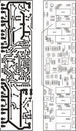
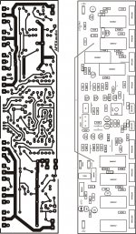
Idea full complementary simetry for minimized distorzion and posible oscilation.Design use lokal feedback and minimum compezation for low TIM. This concept sound beter to me than unsimetry design with quasy complementary output stage useing only N-tip mosfet like IRFP250. IRFP250 have no P-tip complement (IRFP9250 for example) and that was reason not use them. I use IRFP250 in D class amplifier.Would you happen to have a schematic that contains the component values? Also, what are your thoughts on using the IRFP250 instead of the 240?
H class amplifierhi apexaudio
greetings what is the output power of the h class amplifier using 2sc5200 2sa1943 and irf 2807 any schematic please nice mosfet amplifier
thanking you
andrew lebon
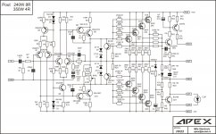
Pout 480W 8R, 750W 4R
H class amplifier is stil in comercial use. I post schematics when he was remain with new driver model. I will post schematic of older version H class amplifier with NE5532 in iput stage and IR2117 for driving step mosfets.
Redrawing mistake. 2N5551 and 2N5401 wrong notification, corect on this schematics. 2SC2383 replaced with MJE340, 2SA1013 replaced with MJE350 in newer version both are OK. 2SB861 and 2SD1138 in VAS can be used too.
Attachments

Last edited:
Hi Apex, i dont think your vas is unusal, its a cfp, I use it in alot of my amps, what is unsual is the your temp compensatiom circuit, Im still guesing how it could work.
The thought has come to mind that the cfp transistor that gets mounted on the heatsink has something to do with it but Id have to build it to see the exact effect.
The thought has come to mind that the cfp transistor that gets mounted on the heatsink has something to do with it but Id have to build it to see the exact effect.
My best suggestion
Dear Apex, Please take time to try this. Tie a 1000µF capacitor between the emitter of Q9 to the emitter of Q10. I truly believe this will really clean up the highs even though the amp sounds good now.
Now a question, why are the gate resistors of the output FET 470 ohms? It seems to me I have measured this device and its impedance is 50 ohms so a gate resistor of 50 ohms would make more sense to me. This may cause some other problem and if you do not feel like taking time to answer that is fine. No insult is intended!")
Redrawing mistake. 2N5551 and 2N5401 wrong notification, corect on this schematics. 2SC2383 replaced with MJE340, 2SA1013 replaced with MJE350 in newer version both are OK. 2SB861 and 2SD1138 in VAS can be used too.
Dear Apex, Please take time to try this. Tie a 1000µF capacitor between the emitter of Q9 to the emitter of Q10. I truly believe this will really clean up the highs even though the amp sounds good now.
Now a question, why are the gate resistors of the output FET 470 ohms? It seems to me I have measured this device and its impedance is 50 ohms so a gate resistor of 50 ohms would make more sense to me. This may cause some other problem and if you do not feel like taking time to answer that is fine. No insult is intended!
Hi Apex, i dont think your vas is unusal, its a cfp, I use it in alot of my amps, what is unsual is the your temp compensatiom circuit, Im still guesing how it could work.
The thought has come to mind that the cfp transistor that gets mounted on the heatsink has something to do with it but Id have to build it to see the exact effect.
I suspect the temperature compensation is non-obvious. Maybe D1 D2 D3 and D4 slight increase in temperature decreases bias current through the differential pairs (x20 as that is the gain of that section) which tends to turn off Q7 Q8 Q9 and Q10 limiting bias. This seems plausible as 1N4148 are very sensitive to any temperature change having very low thermal mass and change temperature even from radiant energy. If this thing was all in a box I am willing to bet it has a negative temp of bias due to this effect.
This is very easy to test. Use freeze spray on the diodes and watch the bias for big changes. This "theory" will quickly prove right or wrong.
Sory, I dont speak English, is hard to me to replied becouse I dont understend question or sugest sometimes, I hope my tone will be beter in future.
dont worry about it, likely its partially my interpretation too.
I dont use this PCB in a last 2 year (repleced with H class in PA and A class for home aplication), but I must build couple PCBs again and try to see the effect on some sugestion.Hi Apex, i dont think your vas is unusal, its a cfp, I use it in alot of my amps, what is unsual is the your temp compensatiom circuit, Im still guesing how it could work.
The thought has come to mind that the cfp transistor that gets mounted on the heatsink has something to do with it but Id have to build it to see the exact effect.
Hvala zemljak, potrudio sam se. Mada lose mi ide pisanje na Engleskom, pola ih nerazumem, na Srpskom bi napisao roman o ovom pojacalu. Ugradio sam preko 120 modula, sema je zahvalna, stabilna i besumna. Mirna struja se cak blago smanjuje kako se pojacalo greje, a koliko sam razumeo neki neveruju da to uopste moze da radi. Neko je pomislio da ja to hocu da prodajem. Ja ovo pojacalo vise ne radim, ali mogu da preporucim svakome. Ovakav dizajn ne zastareva kao ni lampe. Meni za PA trenutno vise odgovara H klasa zbog vece snage i manje grejanja, a i 2SA1943/2SC5200 imaju veci probojni napon.Nice work, Mile
Pozdrav
Mile, prijavi se na diyaudio.rs - tamo smo svi iz Srbije kao i ovde, ali je sve na srpskom, otvori ovu istu temu i tamo pa da se raspricamo (tamo mi je nick sipi). Citamo se !
P.S. Nemoj ovde da pises na srpskom, nije po pravilima foruma
Apexaudio is not a guy with an "attitude", he is just having great difficulties understanding english. He is not selling this amp and he is not even making it any more (he went for class H with BJTs). This amp is his contribution to the forum as proven and thermally/electrically stable design which was reliably used in PA for more than a decade.
Yes, that my profile at diyaudio.rs
Dear Apex, Please take time to try this. Tie a 1000µF capacitor between the emitter of Q9 to the emitter of Q10. I truly believe this will really clean up the highs even though the amp sounds good now.
Now a question, why are the gate resistors of the output FET 470 ohms? It seems to me I have measured this device and its impedance is 50 ohms so a gate resistor of 50 ohms would make more sense to me. This may cause some other problem and if you do not feel like taking time to answer that is fine. No insult is intended!
Hi
A cap between emitter of Q9 and emitter of Q10 provides AC coupling between the OPT gates and allows the negative driver to discharge the positive mosfet gates and vice versa. At low frequencies, the charge required to drive the mosfet gates is very small, but for higher frequencies it is significant. Vgs increases for higher output conductance so when the current falls back to the zero crossing, the extra charge must be sucked out or cross conduction may happen at higher frequencies, creating some Gm doubling and distortion. To me, this distortion sounds a bit like crossover distortion. Also bias of the output stage should be high enough to counter the transconductance droop of the fets so it becomes more constant WRT current. This helps to reduce crossover distortion, probably somewhere around 150-250mA.
470R does seem a bit high for gate stoppers. Have you ever considered using a Zobel filter on each OPT gate? This allows you to control the frequency roll off more accurately than just a gate stopper alone. Of course PCB layout and proper grounding is very important.
Q7 & Q8 bias is 600uA + a couple hundred uA of base current. This seems a little light for MJE350. Perhaps you could consider bumping it up to a couple mA and use a small signal device with higher Ft and lower Cob. Q9/10 does not require enough base current to warrant a med pwr device for Q7/8, IMHO.
With a small signal VAS transistor, you may be able to reduce that huge 100pf phase lag compensation cap that is swamping away all of your BW, considering the output Z of the input stage.Hi apex i am impressd your mosfet amp desin but i dont know your h class circuit please informaition khalsaaudiocenter@yahoo.com
H class amplifierHi apex i am impressd your mosfet amp desin but i dont know your h class circuit please informaition khalsaaudiocenter@yahoo.com
Pout 480W 8R, 750W 4R
H class amplifier is stil in comercial use. I post schematics when he was remain with new driver model. I will post schematic of older version H class amplifier with NE5532 in iput stage and IR2117 for driving step mosfets.
- Home
- Amplifiers
- Solid State
- MOSFET Amplifier IRFP240/IRFP9240