An externally hosted image should be here but it was not working when we last tested it.
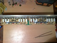
Apex as i promised i have uploaded photo of amp
")
Later im going to make more photos, but first i need to fix that ifps's blowing problem.
Power suply is being used from montarbo active monitor +/-75v 2.1A(per rail) +2x10.00o0uf.
It's nothing against your design skills at all but don't you think amps like this are a lot of effort and money when you can get more power and performance from a chip like the LME49830 and a pair of Double die FETs on a board a quarter of the size?
What I mean is, are were gettin anything more out of big amplifiers like this opposed to smaller new ones?
What I mean is, are were gettin anything more out of big amplifiers like this opposed to smaller new ones?
harizhent
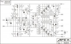
What transistors have you used in TO92 ,are those 2SA/2SC or a 2N transistors? PCB was designed for a 2SA/2SC and if you used 2N5551 / 5401 like i did,than you shuld pay attention in a pin-placements,they are NOT THE SAME! One more thing,i did this amplifier and it worked right away,only thing i did later was replacing 500R trim. with 1k to acchive 40mA per output pair. I used schematic from below,and it works just like it should-loud and clear!
What transistors have you used in TO92 ,are those 2SA/2SC or a 2N transistors? PCB was designed for a 2SA/2SC and if you used 2N5551 / 5401 like i did,than you shuld pay attention in a pin-placements,they are NOT THE SAME! One more thing,i did this amplifier and it worked right away,only thing i did later was replacing 500R trim. with 1k to acchive 40mA per output pair. I used schematic from below,and it works just like it should-loud and clear!
Attachments

harizhent - pay attention how all TO92 transistors are placed and before mounting them take a look where is B/C/E on a pcb,than where are they on a transistor that you are about to mount on a pcb. That is the only safe way to have a succesfull first plugging in. Try to match as best as you can Q1,Q2-Q4,Q5 to get lowest possible dc-offset. One more thing,do not forget to put gnd from psu to an input cable as on all APEX amplifiers!
Boscoe,i am just a beginer and don´t know much about amplifier in theory,however in this http://www.ti.com/lit/ds/symlink/lme49830.pdf pdf there is a schematic but the output is with IRFP240 / 9240,so the LME49830 just drives them,and it does not get this power it self alone. Also,on schematic given in a pdf there is only one pair of IRFP,and there is no much chance that it will give as much power as let´s say APEX HV23 or any other power amplifier with 4 pairs of output transistors-at least for more than a few micro-seconds!
Boscoe,i am just a beginer and don´t know much about amplifier in theory,however in this http://www.ti.com/lit/ds/symlink/lme49830.pdf pdf there is a schematic but the output is with IRFP240 / 9240,so the LME49830 just drives them,and it does not get this power it self alone. Also,on schematic given in a pdf there is only one pair of IRFP,and there is no much chance that it will give as much power as let´s say APEX HV23 or any other power amplifier with 4 pairs of output transistors-at least for more than a few micro-seconds!
Did you use bc327/337 or a bc639/640? I´d say that it is too thick and that there is poor heat transfer to a heatsink. Also,you should do something about hole edges,that aluminium around hole edge could do some electrical connection and also damage to an output transistors. All of those are just guessing and suspicions... You never said how did those blown up,immediately or after some time?
Attachments
Last edited:
Did you use bc327/337 or a bc639/640? I´d say that it is too thick and that there is poor heat transfer to a heatsink. Also,you should do something about hole edges,that aluminium around hole edge could do some electrical connection and also damage to an output transistors. All of those are just guessing and suspicions... You never said how did those blown up,immediately or after some time?
You are asking if i was using Bc639/640 for Q11/12? No, im using 2sa970/sc2240.
I have checked if there is any connection between heatsink and mosfets...there was no..
Modfets started poping like popcorn at the same time with the fuse(witch is soldered under the pcb to +75v rail...), just after bias voltage reached 17mV.. i just pluged in, adjusted bias voltage to 30mV and it started falling to 17mV and after few seconds... PEW ... One pair and fuse is gone. All blown mosfets are like shorted...
Did you check how much did they got heated before blowing up? Those transistors that you have used have higher operation voltage but three times less power and ten times less current allowed to run through. I can´t say for sure that it is because of them,but also i don´t know why haven´t you used BC639-640 when they are suggested in schematic?
44250 i just changed Q11 and Q12 to BC640/639 like in your post posted circuit
as i see the only difference between this schematic and schematic posted in apexaudio 470 post is these transistors?
i had tried to setup bias.. but after 10sec irfp240's got very hot. on start amps emits a lot of noise. And again voltage on 0.47r resistors from start started falling from ~2v to 20mv and started riseing again(had to turn of, because irfps got hot).
I don't know what to say,i don't have enough of knopwledge... Does the heatsink get hot along with irfp-s? The only thing that i could help you is to take a good look at pictures of what you did so far. Take a few detailed pictures from above and the bottom of a pcb,maybe you are overseeing always the same thing-that happens to me quite often and something that i don't see at all to someone else is very obviously. This amplifier works,you could se my videos on youtube... One more thing-you should use some safety measures and that would be two about 20w and say 20-30 Ohm resistors,each in series with power supply rails / or a light bulb in series with transformer primary . Both measures will protect output transistors.
who corrupted APEX sch?
Has someone corrupted APEX schematic shown in post573?
I see a resistor bias for the output stage and I see Vertical mosFETs in the output stage.
Is this a ClassB amplifier that is designed that it can never run warmer than cold?
Or is it supposed to be a ClassAB amplifier, in which case the resistor biasing is completely wrong for a vertical mosFET output stage.
I did it like in post 565,only i used 1k trim instead 500R to achive about 40mA bias per pair warmed up to a 30°C . I haven't abused it yet because PSU is waiting for 30000uF per rail for both channels. Now it works with only a pair of old 6800uF. Not sure what you ment to say(i must learn a lot more),but i hope that APEX will say a word or two. Up to 100 watts amp works really nice,i hope to test it at full 250w 8r when capps become a part of it.
Last edited:

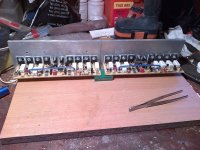
I think this one should work.
Two missing pairs are blown away
With good thermal connection mosfets with heatsink only heatsink can be warm after 10min, mosfets can't be hot after few seconds.
Has someone corrupted APEX schematic shown in post573?
I see a resistor bias for the output stage and I see Vertical mosFETs in the output stage.
Is this a ClassB amplifier that is designed that it can never run warmer than cold?
Or is it supposed to be a ClassAB amplifier, in which case the resistor biasing is completely wrong for a vertical mosFET output stage.
This is class AB amplifier, bias is overcompensated and always drop when amp get warm. Amp can work in class A with lower rail voltage and large heatsink if you want.
- Home
- Amplifiers
- Solid State
- MOSFET Amplifier IRFP240/IRFP9240