under the URLyes, the values are little different (between 676 and 683 mR). But to little for the observated variation at idle current.
While upload the updated schematics I get this message:
413 Request Entity Too Large
what is the reason ?
How do I upload images or files? | diyAudio Helpdesk
I read:
Please note that in the attachment window you will find a list of the allowed file types
and their maximum sizes. Files that are larger than these sizes will be rejected.
This means, I need apps resp. tools for reducing data before upload.
Nevertheless - until recently I could easily upload jpg-files up to 10 MB without trouble (I even used diyaudio.com for quick data reduction of various jpg files for other applications).
What is happen on diyaudio in the upload area?
Last edited:
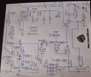
the showed circuit are to find in the datasheet of AD844The Input stage is a heavily cascoded symmetrically realized buffered current feedback input stage, which couples into a high linearity push pull current mirror ("VAS").
If you take a look into classic CFB-OPAs like AD844 or AD846 you'll see very similar circuitry.
The basic topology is the one of a transimpedance stage (input + mirror) and a power buffer.
http://www.analog.com/media/en/technical-documentation/data-sheets/AD844.pdf
on this circuit even the non inverted input has low impedance - in opposite of the AD846 and the used circuit in OMTEC's CA25 - go to
http://www.analog.com/media/en/technical-documentation/obsolete-data-sheets/270284AD846.pdf
Where is a successor of the AD846 ??
Check out also this application note:
http://www.ti.com/lit/an/snoa725a/snoa725a.pdf
Last edited:
Hi,
thanks.
I understand the AD 846 schematics: But: For me, the Omtec has a high impedance input and current feedback.
And I see a cacoded amplifying stage, but no output buffer. Correct?
I would be happy, if someone posts the control circuit with some explanation.
Regs, Dirk
thanks.
I understand the AD 846 schematics: But: For me, the Omtec has a high impedance input and current feedback.
And I see a cacoded amplifying stage, but no output buffer. Correct?
I would be happy, if someone posts the control circuit with some explanation.
Regs, Dirk
No.Hi,
thanks.
I understand the AD 846 schematics: But: For me,
the Omtec has a high impedance input and current feedback.
And I see a cacoded amplifying stage, but no output buffer. Correct?
I would be happy, if someone posts the control circuit with some explanation.
Regs, Dirk
There is an input buffer (T1 and T2, thus high impedance input) for the actually non inverted input (base T3, T4) and a darlington output buffer (T33/T34 include the associated power BjT devices - 6 pcs in TO-3 outline) behind the cascoded VAS stage (T9+31/T10+32).
Because the NFB signal was flow in the emitters of T3/T4 (= inverted amp) we call this NFB kind "feedback with current control" (in opposite to a typical LTP input amp with differential amp and two high impedance inputs).
Basically, but not in all details the same circuit than the internal circuit of AD846.
The reason for multiple cascoding at the input stage could be reducing "Memory distortion" - go to
Memory Distortion Philosophies - Part 1 : Theory
Lavardin Technologies audio systems
Lavaradin Amp and "Memory distortion"...
Memory distortion, crap or serious?
Last edited:
Owner's Manuals (Instruction Manuals) wanted from all Versions
There are at least three different versions - go to
Bedienungsanleitungen
But I have found only the attached version.
Who can upload the other two ?
There are at least three different versions - go to
Bedienungsanleitungen
But I have found only the attached version.
Who can upload the other two ?
Attachments
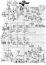
There rises up new questions arround the voltage regulator - go to
http://www.diyaudio.com/forums/powe...c-power-amplifiers-ca25-ca60.html#post5285841
http://www.diyaudio.com/forums/powe...c-power-amplifiers-ca25-ca60.html#post5285841
OMTEC CA60V3 schematic wanted
I will get the last version (PCB from Feb 2005) for troubleshooting next time. Maybe anybody have the schematics for upload - thank you very much in advance.
check out this URL for owner's manuals:
Bedienungsanleitungen
I will get the last version (PCB from Feb 2005) for troubleshooting next time. Maybe anybody have the schematics for upload - thank you very much in advance.
check out this URL for owner's manuals:
Bedienungsanleitungen
Attachments
-
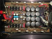
 Omtec CA60V3 Kendeil-Elkos-III.jpg1 MB · Views: 334
 -
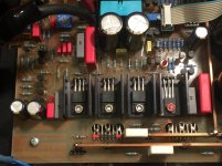
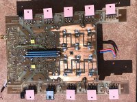 OMTEC CA60V3 Power Amp solder side.jpg1.1 MB · Views: 351
 -
 OMTEC CA60-V3 Protect-III.jpg1 MB · Views: 184
 -
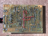 OMTEC CA60V3 Protect solder side-III.jpg1.1 MB · Views: 244
 -
 OMTEC CA60V3 Power Amp PCB top-II.jpg830.2 KB · Views: 178
 -
 Omtec CA60V3 Kendeil-Elkos.jpg135.4 KB · Views: 164
 -
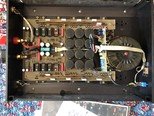 OMTEC CA60V3 open.jpg10.1 KB · Views: 166
 -
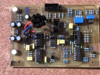
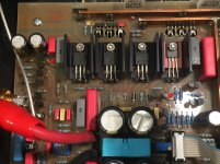 OMTEC CA60V3 Driver-Stage-I.jpg654.6 KB · Views: 169
 -
 OMTEC CA60V3 Driver-Stage-II.jpg637.2 KB · Views: 183
 -
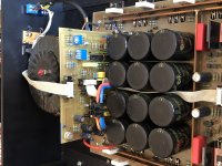 Omtec CA60V3 Kendeil-Elkos-II.jpg908.9 KB · Views: 151
Last edited:
In this case this paper is of interest:The Input stage is a heavily cascoded symmetrically realized buffered current feedback input stage, which couples into a high linearity push pull current mirror ("VAS").
If you take a look into classic CFB-OPAs like AD844 or AD846 you'll see very similar circuitry.
The basic topology is the one of a transimpedance stage (input + mirror) and a power buffer.
Evolution of High-Speed Operational Amplifier Architectures
https://pdfs.semanticscholar.org/f0b1/73d0f261554b3a7d73c370db303c27240c85.pdf
Last edited:
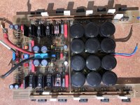
Here an additional service report from a German forum
Omtec CA-25 Class A Monoblock
Omtec CA-25 V2 Class A Monoblock
In the moment I am looking for an appropriate main switch (toroidal transformer without inrush current limiter)
The genuine main switch looks like this under
RS PRO DPDT Toggle Switch, Latching, PCB | RS Components
and in my opinion it is too weak to switch on toroidal transformers.
Are there 20-40A switches in this outline resp. sizes ?
In the right A value the dimensions are significantly larger
https://eu.mouser.com/ProductDetail/NKK-Switches/S422/?qs=FyOeoOG5V0rhKzVp3zHW2A==
and
S732 NKK Switches | Mouser Europe
https://eu.mouser.com/datasheet/2/295/stoggleshighcap-1663465.pdf
(unfortunately obsolete).
Last edited:
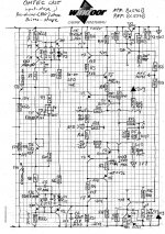
- Home
- Amplifiers
- Solid State
- Omtec Mono Power Amplifier "CA 25" (CA25) - Schematic wanted