This change brings another problem: it is extremely sensitive to reactive loads. This is a well known disadvantage of voltage feedback.
The actually measured harmonics ( when driving a speaker w/o crossover ) is even better than the sim. However I am a bit suspicious on the accuracy of a demo of a harmonics analyser...
The actually measured harmonics ( when driving a speaker w/o crossover ) is even better than the sim. However I am a bit suspicious on the accuracy of a demo of a harmonics analyser...
Last edited:
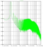
Another modification: replace the CFPs at the output with power Darlingtons - some minor modifications to the biasing are required, but the sonics are just as good as the CFP version. The THD20 FFT shown below is for ~27V amplitude into 8 ohms. It's even better at low swings, where H2 is head and shoulders above everything else.
Edit: With Sanken Power Darlingtons and higher rails, this should be brilliant!.
Edit: With Sanken Power Darlingtons and higher rails, this should be brilliant!.
Attachments
Last edited:
The power is determined by Vcb of Q2. As long as Q2 is not saturated ( Vcb >0.35--0.6volt) everything is fine. I have been testing this configuration as well. It has the big disadvange of reactive distortion. This is all due to voltage feedback.
A complex load shifts the phase between voltage and current. Voltage feedback performs
a voltage to current transformation and this results in Q2 being saturated even at low power. This does not happen with current feedback so one has to implement current feedback i.e. emitter resistors. That is the design trick to modify Vish is a "merge" of voltage and current feedback. Otherwise the Vish amp cannot drive any speaker box with crossover.
Another modification: replace the CFPs at the output with power Darlingtons - some minor modifications to the biasing are required, but the sonics are just as good as the CFP version. The THD20 FFT shown below is for ~27V amplitude into 8 ohms. It's even better at low swings, where H2 is head and shoulders above everything else.
Edit: With Sanken Power Darlingtons and higher rails, this should be brilliant!.
Let me explain:
a BJT is a current amplifier. Thus there has to be ONE and only one point where voltage is converted to current. In Vish topology this is the Rush cascode.
Hence the "result" of voltage to current must be controlled with current, not voltage. That would introduce a second point of voltage to current conversion.
In terms of MOSFET the voltage to current conversion takes place in the last stage. Thus there can be reasonable doubt whether Lin topology is optimal for MOSFET in the last stage.
In our case a combination of tube - or FET only predriver ( voltage amplifier)
would possibly be the optimum.
Ok. I replaced the fast 2SC5200 with 10 MHz types and the 2SA with ( very old) BD390
specified 50 Mhz and wow! no more latchup. The amp produces up to 30 volts (!) p
with still less than 0.8% thd into 6 ohms . Up to 40 watts the harmonics spectrum is absolutely perfect. Further after a 5 sec duration burst at max dissipation (2/3 max power) the quiescent current is unchanged at 15 mA. It appears the problem could have been tackled with a more tricky compensation leaving the modern fast BJTs.
Well after all...a close to perfect amp.
i don't like Darlingtons... but a discrete Darlington configuration is certainly worth to consider. Remember the Achilles heel of this topology is reactive distortion. For my purpose active speaker this is not an issue as long as the speaker operates above resonant frequency and is hence inductive. The amp still has problems with a vented speaker box where the impedance swings from capacitive to real to inductive impedance.
I thought that with increasing frequency a falling impedance indicates inductive loading and that rising impedance indicates capacitive loading.speaker operates above resonant frequency and is hence inductive.
Above resonance you usually find that with increasing frequency that initially the impedance falls (inductive) and then rises (capacitive).
The inductive portion (falling impedance with rising frequency) is usually between one and two octaves.
I use the electrical equivalent of a electrodynamic speaker as derived by Paul Klipsch.
The important part of it is the electrical representation of the radiation resistance.
For a midrange 4" this impedance is capacitive below 300/s and is real from 500/s upwards.
So we have to consider the compliance of air ( and speaker) which is represented as inductor , in series with the real radiation resistance. This gives for a particular speaker
0.7 mH in sries with 6 ohms above 300/s.
Ideas:
1) Current mirror with the LTP? Probably not worthwhile - it will improve THD20, but will also kill H2 and the desirable sonics. It will require 2 additional matched active devices.
2) Replace one of the two MUR460 silicons with a Schottky rectifier - the combined drop is a bit lower, and closer to that of a Darlington. During cross-over commutation, there should be less high-frequency 'hash'.
3) Snubber the rectifier chain with a 47nF/100nF foil cap (already done).
4) Flip the entire modified Visch output stage over to use NPN darlingtons instead of the PNPs shown. They're better spec'ed and less expensive than equivalent P-darlingtons.
5) Switch from bootstrapped VAS to current-source load (probably not really useful except for deep bass response).
(The CFP outputs are more tunable, since the upper half can be tuned independently of the lower half. But that comes at some cost in circuit complexity. When I eventually build this, I'll probably go with integrated Darlingtons, despite poor SOA compared to discretes.)
According to my results a Schottky increases the odd harmonics. I have no idea why but it is significant. A fast silicon with a 100nf parallel on theo other side reduces higher odd harmonics.
5 is important the source impedance of VAS is a fine tune of the harmonics spectrum.
Normally I avoid current sources. They make some sense in a jFET LTP BJT cascode.
The preamp I have posted appears very suitable as its harmonics are the same as of the amp. As its output impedance is about 50 ohms, a series resistor does a simple job of fine tuning.
According to my results a Schottky increases the odd harmonics. I have no idea why but it is significant. A fast silicon with a 100nf parallel on theo other side reduces higher odd harmonics.
I agree, considering that now there are ultrafast silicon diodes with TRR of around 20ns.
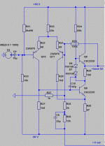
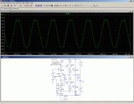
Here is the complete schematics with VAS. The Q5 Q7 2SD718 are not suitable as SOA is too small but their fT is right and also hfe(f) . Further BD390 are no longer made but again
fT and hfe are right. The amp achieves at 28 Vp into the simulated speaker load a thd <0.02% with odd harmonics all 30dB below even. Even at full output swing the respective non conducting transistors ( in class B) are conducting the min current
is about 10 mA.
An integrator will be added that keeps the dc out component in the mV range, it feeds the non inverting input.
Attachments
Last edited:
since you want a current feedback, why not this one ?...
with about 600 mA quiescent current, it display
exceptionnal performances...
yes, this actually very common topology sounds indeed really good -
author and developer of the "Black Devil" was Gerhard Haas, Owner of
EXPERIENCE electronics - Home -
especially by enhanced idle current of power buffer stage.
Additional enhance of sonic quality you will get either through enhancing the quiescent current of the input transistor (in the presently geniue topology <<1mA) or by replace the input transistor through a jFET (better characteristic by lower currents than small signal BjT's).
LTspice can provide tone bursts in a number of ways:
Here is one.
Picture 2 shows the detail, and picture 3 shows also the voltage across the capacitor.
It is, because the level of charge of the capacitor (which sets the quiescent current) relies on the splitting factor of the switching modulator formed by D1, Q2 and Q7.
When the average level of conduction of Q2 increases, the duty cycle of D1's conduction also increases, diverting the 15mA bias away from Q7 more of the time.
This decreases the charge going into C1, and corrects the Iq through Q2 (and Q1).
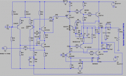
By the try to get simulation results of the Visch topology I haven't success, because the long tailed input pair don't conduct.
Is the paper with the complete article here posted (Wireless World, April 1975, p166)? Schematic and shortform desribtion is to see about post #7.
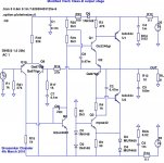
What have I overlooked (have a look to the attachement) ?
Unfortunately I don't see DC values by all simulation results here.
Attachments
Last edited:
Please let me know the Electronic World edition and launched year, where this circuit is inside - thank you.Here is another non switching circuit
I recall, the developers of this circuit comes from
University of Twente - University of Twente
By the try to get simulation results of the Visch topology I haven't success, because the long tailed input pair don't conduct.
Is the paper with the complete article here posted (Wireless World, April 1975, p166)? Schematic and shortform desribtion is to see about post #7.
What have I overlooked (have a look to the attachement) ?
Unfortunately I don't see DC values by all simulation results here.
I see a number of problems in your sim: first there is an error in the schematic: the emitter of Q7 must be connected to the anode of D1.
Then, I see that Q4 has -38.5V on its base and -88nV on its emitter. That's impossible, there must be something wrong with your model of the BCP53.
And I found that the Visch topology is prone to latch-up, both in simulation and in reality.
To make it work in sim, I had to force an initial condition on the collector of Q7 (Vn009): -1.69V.
Attachments

Thank you for this advices. The model of BCP53 is approx. the same than BD140 and in all other circuits it works without trouble.I see a number of problems in your sim: first there is an error in the schematic: the emitter of Q7 must be connected to the anode of D1.
Then, I see that Q4 has -38.5V on its base and -88nV on its emitter. That's impossible, there must be something wrong with your model of the BCP53.
And I found that the Visch topology is prone to latch-up, both in simulation and in reality.
To make it work in sim, I had to force an initial condition on the collector of Q7 (Vn009): -1.69V.
The not present connection between the emitter of Q7 and the anode of D1 was definitely an error from me. But after correction that, no change in results and behavior was to observe.
The input stage about
4QD-TEC: Low distortion Audio amplifier
looks familiar with the Visch amp input. Perhaps this will help to find the actually reason for not correct simulation results.
One error now I have found: the voltage at the base of Q6/5 cannot be the same. That must differ at least 1,3 volts.
The cathode of D2 seems to be also wrong connected - there must be 2 diodes in serial and connected to -15V by R8. Otherwise flows the ref current about the B-E direction instead aboput the diode(s)
Is it possible to show the dc conditions in your simulation?
Last edited:
- Status
- This old topic is closed. If you want to reopen this topic, contact a moderator using the "Report Post" button.
- Home
- Amplifiers
- Solid State
- Class B w/o crossover distortion (1975)