Gentlemen,
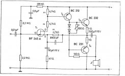
This circuit was published in the "FET Cookbook" (Das FET Kochbuch) written by the Texas Instruments application guys, back in the seventies (as far as I know it was not published in English). The question I have is not about the audio qualities of the design but the function of the 4.7 KOhm resistor connected between the drain of the FET (T1) and the base of the BC212 driver (I marked it as R2).
Apart from the possibility of eliminating a large surplus of 4.7 K resistors in the lab, I really honestly cannot see any reason for including it in the circuit but somehow I cannot imagine that the guys at TI would have put it in without a good reason, so I was wondering if you have any ideas.
At the 200 uA-ish drain current the FET is operating at, its output impedance is very high (above 100 kOhm) so the 4.7 K in series hardly makes any difference. I can't see it would make any difference from a DC biasing point of view either, but then what is it for?
I must confess I'm baffled. The rest of the circuit makes sense.
Thanks for any suggestions.
Attachments
Gentlemen,
This circuit was published in the "FET Cookbook" (Das FET Kochbuch) written by the Texas Instruments application guys, back in the seventies (as far as I know it was not published in English). The question I have is not about the audio qualities of the design but the function of the 4.7 KOhm resistor connected between the drain of the FET (T1) and the base of the BC212 driver (I marked it as R2).
Apart from the possibility of eliminating a large surplus of 4.7 K resistors in the lab, I really honestly cannot see any reason for including it in the circuit but somehow I cannot imagine that the guys at TI would have put it in without a good reason, so I was wondering if you have any ideas.
At the 200 uA-ish drain current the FET is operating at, its output impedance is very high (above 100 kOhm) so the 4.7 K in series hardly makes any difference. I can't see it would make any difference from a DC biasing point of view either, but then what is it for?
I must confess I'm baffled. The rest of the circuit makes sense.
Thanks for any suggestions.
Yes it is funny. The only think that comes to my mind right now is that it may have a function in overload prevention or overdrive recovery. What's the supply voltage? It may limit the max current in the FET at overdrive.
jd
The resistor will limit the current as the 50 uF cap charges up.
Yes that seems a good reason for it.
jd
As far as I know, that resistor is decreasing open-loop gain but I don't really see the point for that.
I don't think it (R2) does anything on the gain.
jd
Gentlemen,
This circuit was published in the "FET Cookbook" (Das FET Kochbuch) written by the Texas Instruments application guys, back in the seventies (as far as I know it was not published in English). The question I have is not about the audio qualities of the design but the function of the 4.7 KOhm resistor connected between the drain of the FET (T1) and the base of the BC212 driver (I marked it as R2).
Apart from the possibility of eliminating a large surplus of 4.7 K resistors in the lab, I really honestly cannot see any reason for including it in the circuit but somehow I cannot imagine that the guys at TI would have put it in without a good reason, so I was wondering if you have any ideas.
At the 200 uA-ish drain current the FET is operating at, its output impedance is very high (above 100 kOhm) so the 4.7 K in series hardly makes any difference. I can't see it would make any difference from a DC biasing point of view either, but then what is it for?
I must confess I'm baffled. The rest of the circuit makes sense.
Thanks for any suggestions.
This resistor (by your circuit in the drain line) I must often introduce in amps, that I have for service to reduce the C-E (D-S) voltage (and loss power) about the first gain stage transistor (if there are differential amp then two resistor must be introduce).
Especially in such cases, if the whole amplifier runs with supply voltages above 100 volts. NAD's integrated amplifier 3240PE is a good example - please look to the PCB hot spot (black PCB) arround the LTP (2x 2SC2240 differential input amp). After introduce the appropriate resistors in the collector lines the thermal loss is much lower (only 20 degrees above ambient temperatur).
An additional advantage is now the use of normal 30V small signal types like BC559C (or BC549C - according the circuit) independend of the individual used voltage supply.
Last edited:
tiefbassuebertr,
This was my first thougt too, but the voltage drop is too small, only about 0.6V, in this case to have that function.
Neither do I think it is to limit the current to charge the capacitor. The current is already very small, due to the R1.
And no it has no impact on the voltage gain since the voltage is not used by T2.
Member
Joined 2009
Paid Member
The 70's, that was right in the middle of the Cold War. It was a practice to introduce strange technical items that had no purpose but would tie-up the other guys scientists for years trying to figure it out.
Keep trying to figure it out guys !
this resistor role is logic, as explained earlier in the thread..
without it, there would be circumstances where the fet could
stand high currents that would destroy it...
if the drain was connected directly to the bjt base, impulse current
would be limited only by the source resistor connected to the
capacitance that goes to ground..
since the value of this resistance is very low and as it
define the closed loop gain, the current must be limited in the
other side of the fet, in the drain circuit, using this
"mysterious" resistance...
A curiosity - no one mentioned the 120 ohm resistor between the base of t4 and the hot side of the load. Kind of a bootstrap circuit, but why send your voltage gain current through the load, unless some kind of bias for the load was desired? My guess is that this circuit was a drawn but not tested. Has anyone tried to simulate it?
<snip> My guess is that this circuit was a drawn but not tested. Has anyone tried to simulate it?
That's a pretty big swag.
 In my experience with the semiconductor industry (I designed semiconductor ATE in a past life) I am almost certain that TI would not have published an untested design - does not mean it is the ultimate performer perhaps, but I can almost guarantee it will work.
Consider another possibility, R1/R2 reduce open loop gain by at least 6dB in addition to the other possibilities discussed here..
Last edited:
Gareth,
You just gave the most credible explanation for the magical mystery resistor: enemy deception. I really like it.The 70's, that was right in the middle of the Cold War. It was a practice to introduce strange technical items that had no purpose but would tie-up the other guys scientists for years trying to figure it out.
The 70's, that was right in the middle of the Cold War. It was a practice to introduce strange technical items that had no purpose but would tie-up the other guys scientists for years trying to figure it out.
Keep trying to figure it out guys !
Well, it may keep us busy, but I doubt that it would keep 'the other guys scientists' busy for more that 100mS or so
I mean, it's not that this secret amp would revolutionize warfare....
jd
Consider another possibility, R1/R2 reduce open loop gain by at least 6dB in addition to the other possibilities discussed here..
I don't see how. R1 is paralleled by the low Rbe of T2. It looks to me like it's just there to set DC conditions of T2, which is a current source. R2 looks like it limits the base current of T2.
- Status
- This old topic is closed. If you want to reopen this topic, contact a moderator using the "Report Post" button.
- Home
- Amplifiers
- Solid State
- Mystery resistor in simple audio amp