the R+C iin the NFB route increases the HF feedback. It has an effect at HF that can improve the phase margin significantly and thus prevent overshoot of fast changing signals.
Overdoing the C or reducing the R can make the amp unstable. It has to be designed carefully and checked thoroughly in the finished amplifier.
Overdoing the C or reducing the R can make the amp unstable. It has to be designed carefully and checked thoroughly in the finished amplifier.
Curiously Doug shows versions of this amp with and without the compensation.
The notes and circuit diagram that accompany the PCB's show beyond doubt a value of 100pf.... which if you try that will make the whole thing oscillate. The original article doesn't "mention" this network either but shows them... odd.
The notes and circuit diagram that accompany the PCB's show beyond doubt a value of 100pf.... which if you try that will make the whole thing oscillate. The original article doesn't "mention" this network either but shows them... odd.
I have that circuit in front of me from Dougs audio power handbook 3rd edition 2002 and it's clearly not shown. Same outputs and drivers, but using MPSA42/92 for the signal stages. The original articles in EW have it, the circuit with the PCB's shows 100pf ???
In practice on the proper board it doesn't need it for stability I found but I did fit a 15 pf in the end.
In practice on the proper board it doesn't need it for stability I found but I did fit a 15 pf in the end.
Yes in Book is apparently 15pF/220R (3rd 2002), but in article 2004 16pf/330R ,the output transistors are the sameI have that circuit in front of me from Dougs audio power handbook 3rd edition 2002 and it's clearly not shown. Same outputs and drivers, but using MPSA42/92 for the signal stages..
Which PCB you say, those who had to sell in England?The original articles in EW have it, the circuit with the PCB's shows 100pf ???
.
of the five amplifiers that D. Self shows, only one has the extra NFB components.the handbook shows four complete ClassAB (=Self's ClassB) amplifier schematics.
Two are CFP, one is quasi and one is EF output stage.
The EF shows the feedback modification, the later trimodal and load invariant versions revert to the plain feedback.
The 20W ClassA (EF output) also shows the modified feedback.
Hi, everybody
Now, you can see the PCB of the circuit. In fact, its not exactly Fig.33 of D. Self article, I used some parts of Carlos Destroyer Blameless design (especificaly, the RC circuit that use the D5, C19, R26 and C18 in -VCC; D4, C17, R19, C16 in +VCC).
Tomorrow I will put the circuit correct.
I use DipTrace to do the PCB.
Regards
Ricks
Now, you can see the PCB of the circuit. In fact, its not exactly Fig.33 of D. Self article, I used some parts of Carlos Destroyer Blameless design (especificaly, the RC circuit that use the D5, C19, R26 and C18 in -VCC; D4, C17, R19, C16 in +VCC).
Tomorrow I will put the circuit correct.
I use DipTrace to do the PCB.
An externally hosted image should be here but it was not working when we last tested it.
Regards
Ricks
The PCB was from here... 15 years ago nearly now so might be different. In fact I don't see the Class B listed now.
The Signal Transfer Company
The Signal Transfer Company
The NFB take off point and the output should be on a spur from the main connections between the output transistors. This is one of Doug Selfs "distortion mechanisms" and it is a very real problem.
Haven't studied your PCB in detail but it looks a bit small taking into account some of the components used... the emmiter resistors and output inductor etc. And don't be afraid to make the traces much thicker... when you etch that board it will look very fine print indeed.
Haven't studied your PCB in detail but it looks a bit small taking into account some of the components used... the emmiter resistors and output inductor etc. And don't be afraid to make the traces much thicker... when you etch that board it will look very fine print indeed.
Hi, Mooly
Thanks for helping... well, I used the component from DipTrace and I´m thinking that I need to redesign the pcb because some parts are smaller than reality.
I did not understand "The NFB take off point and the output should be on a spur from the main connections between the output transistors. This is one of Doug Selfs "distortion mechanisms" and it is a very real problem." How can I solve this problem???
Thanks
Ricks
The PCB was from here... 15 years ago nearly now so might be different. In fact I don't see the Class B listed now.
The Signal Transfer Company
Hello Mooly,
Wearing my Signal Transfer hat: interest in the Class B Amplifier faded over time to the point where it was not viable to re-order PCBs in small quantities, so the product was dropped. The card also had an awkward aspect ratio for mounting in a 19-inch case in that it was long and thin.
Class B is, however, not dead
") as design and development continues. Keep an eye on the website! There are a few new things in the pipeline ..... or is it the CAD files....?
as design and development continues. Keep an eye on the website! There are a few new things in the pipeline ..... or is it the CAD files....? Cheers,
Gareth.
Hi, everybody
Thanks for helping, Mooly and AndrewT.
I´ve read the article distortion in Amps, by D. Self. There are a lot of information, so I need a time to processing eeverything!!!
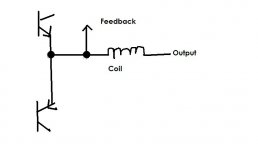
But you are wright! It´s in front of my nose, in fugure 29. And I have another doubt: what is wright??? Look at the picture:
I think tha connection 1 is wrong. Is the same as used in the last version.
The connection 2 is the best choice?
And if I use the connection 3??? In this case, I´m NFB with the signal that was processing by all circuit.
And I forget to link C4, and I´m working on it.
And the last question: I´m in the wright way?
THanks for helping.
Regards
Ricks
Thanks for helping, Mooly and AndrewT.
I´ve read the article distortion in Amps, by D. Self. There are a lot of information, so I need a time to processing eeverything!!!
But you are wright! It´s in front of my nose, in fugure 29. And I have another doubt: what is wright??? Look at the picture:
An externally hosted image should be here but it was not working when we last tested it.
I think tha connection 1 is wrong. Is the same as used in the last version.
The connection 2 is the best choice?
And if I use the connection 3??? In this case, I´m NFB with the signal that was processing by all circuit.
And I forget to link C4, and I´m working on it.
And the last question: I´m in the wright way?
THanks for helping.
Regards
Ricks
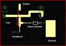
NFB tapping from connection 2 is almost correct.
Move the main thick trace between the emitter resistors to UNDER the output coil//resistor. Take a leg off from this thick trace to the end of the resistor//coil, i.e. towards the output devices. Use this side leg as the tapping for the NFB
Move the main thick trace between the emitter resistors to UNDER the output coil//resistor. Take a leg off from this thick trace to the end of the resistor//coil, i.e. towards the output devices. Use this side leg as the tapping for the NFB
Hi, everybody
Thanks for helpíng.
Wel, I made a new PCB of the Blameless circuit of figure 33 showed in the article:
Distortion In Power Amplifiers
The figures are:


There isn´t jumper in this board.
I would like to know if I can change some capacitors, just because I have another values:
C5, C10 - 220uF -> 470uF
C2 -> 220uF -> 470uF
C4 -> 47uF -> 100uF
And another doubt is:
TR7, TR9 -> 200W power transistor
TR6, TR8 -> 20W transistor
TR13 - 20W transistor
TR12 -> 750mW (Encapsulamento TO-92) (???)
TR5 -> 750mW (Encapsulamento TO-92) (???)
TR4 -> 20W transistor (or can I use a 750mW transistor???)
All resistor are 1% precision.
I´m fixing in the heatsink the TR13 in the center os power transistors. An image show more than 1000 words... I think it is the correct position.

If someone see an error, please, contact me.
I expected you enjoy!
Thanks for helping
Regards
Ricks
Thanks for helpíng.
Wel, I made a new PCB of the Blameless circuit of figure 33 showed in the article:
Distortion In Power Amplifiers
The figures are:
There isn´t jumper in this board.
I would like to know if I can change some capacitors, just because I have another values:
C5, C10 - 220uF -> 470uF
C2 -> 220uF -> 470uF
C4 -> 47uF -> 100uF
And another doubt is:
TR7, TR9 -> 200W power transistor
TR6, TR8 -> 20W transistor
TR13 - 20W transistor
TR12 -> 750mW (Encapsulamento TO-92) (???)
TR5 -> 750mW (Encapsulamento TO-92) (???)
TR4 -> 20W transistor (or can I use a 750mW transistor???)
All resistor are 1% precision.
I´m fixing in the heatsink the TR13 in the center os power transistors. An image show more than 1000 words... I think it is the correct position.
If someone see an error, please, contact me.
I expected you enjoy!
Thanks for helping
Regards
Ricks
- Status
- This old topic is closed. If you want to reopen this topic, contact a moderator using the "Report Post" button.
- Home
- Amplifiers
- Solid State
- Please, help me with Self Blameless