When returning to use the scope plugged to the amplifier i will produce the picture
The amplifier will remain playing music, continuously, over a load or using speaker till wednesday.... soon you will have the picture.
The simulator image is fine, and if i can remember the waveshape was fine too.
Carlos
The amplifier will remain playing music, continuously, over a load or using speaker till wednesday.... soon you will have the picture.
The simulator image is fine, and if i can remember the waveshape was fine too.
Carlos
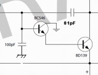
CCS does not create instability. Too much open loop gain with both a current mirror and the darlington VAS is what does it. Use just a low gain BD or MJE340
for VAS with 68 - 100 pf CDOM , all will be good.
OS
not a good idea at all, sorry..
lower gain vas transistor means more current pumped from the
differential, increasing the output DC offset, not to mention higher
THD..better to use vas emitter degeneration and, as as proposed by BV,
with cdom of higher value, 47 to 68 pF , along with getting rid of the
100pf shunt compensation cap, as it s connected on one of the worst
path, in respect of global feedback efficency...
Do it the way you want dear Wahab, but do it instead to go analising
What about to listen?... to hold some soldering iron.....and then you can try several options, the correct and wrong options....you may confirm, giving a nice check up into the theories.
Enjoy the sonics.
regards,
Carlos
What about to listen?... to hold some soldering iron.....and then you can try several options, the correct and wrong options....you may confirm, giving a nice check up into the theories.
Enjoy the sonics.
regards,
Carlos
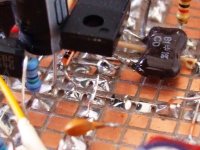
Here you have, i have cutted and continue to play stable, but i will not take the
risk....will solder it once again
it is the one out of focus, the small ceramic one.
But do that in your own amplifiers, install pressing your finger tip over the ceramic and remove it, just bent it to the circuit and return...please, use a non magnetic tool..plastic or wood.
And listen..then return to me to say that i must remove the unit.
Will stay....and check by yourselves, a excelent chance to check some beliefs, rules of thumbs and theories into real life..difference is audible.
regards,
Carlos
Attachments
What about to listen?... to hold some soldering iron.....and then you can try several options, the correct and wrong options....you may confirm, giving a nice check up into the theories.
Enjoy the sonics.
regards,
Carlos
it s already done, carlos...i didn t manage to do better since
1990...i m still sticking with the amp i then designed and built..
i had no simulator at the time, but as i recently simulated it, i found
that it was useless to try to improve it...
must admit that i was very influenced by well known designers, and i
took it as a chance to read their guidelines,as it spared me a lot of time
and deceptions...
regards,
wahab
Fine dear Wahab...in 1990 i started the second marriage
and also started to work to Sony Corporation, sadly was not audio, was Video Professional..but helped me a lot to scape to the audio laboratories in Japan.
One year after the third son born, and i started to became a little bit old, but thinking into the third marriage and one more daugther.
ahahahahahah!
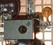
Here is the capacitor, sound was different, and heatsink started to be too much hot....soldered in place once again, with reduce gain and so on, but stable and sounding much better.
Of course was tried from base to colector...but resulted better this way.
regards,
Carlos
and also started to work to Sony Corporation, sadly was not audio, was Video Professional..but helped me a lot to scape to the audio laboratories in Japan.
One year after the third son born, and i started to became a little bit old, but thinking into the third marriage and one more daugther.
ahahahahahah!
Here is the capacitor, sound was different, and heatsink started to be too much hot....soldered in place once again, with reduce gain and so on, but stable and sounding much better.
Of course was tried from base to colector...but resulted better this way.
regards,
Carlos
Attachments
What about to listen?... to hold some soldering iron.....and then you can try several options
You speak to us like we never made any amps?? I built 6 + of these self amps.
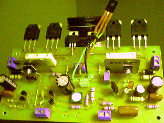
Wahib is right , higher gain is good .. but not too high. In the amp above I finally used a single 2sc3503 (300 gain) instead of EF for VAS with 68p CDOM. 2sc1845/2sa992
(2n5550/5551 will do) as current mirror/LPT ... 80-90db OLG. This is not analysis , this is a real amp that works , daughter is playing games using it NOW...
I also built the same amp as above with bootstrap like your new one and it had better bass but clean highs just like the CCS 'ed VAS (original self amp).
OS
Sorry folks, that capacitor is connected to ground, so, it is a miller spreaded
One to the VAS first stage (100pf) and other to the VAS second stage.
Error into the schematic and will be soon fixed.
That capacitor was never connected to the negative rail.... error into the schematic, my mistake.
The schematic was correct, error was into the board layout i have produced.
regards,
Carlos
Attachments
Last edited:
One to the VAS first stage (100pf) and other to the VAS second stage.
Error into the schematic and will be soon fixed.
That capacitor was never connected to the negative rail.... error into the schematic, my mistake.
regards,
Carlos
the result is the same, safe that connected to ground
it has to stand the full rail voltage rather than 1.2V when connected
to the negative rail...
Here you have folks, the layout fixed with the capacitor in the correct place.
The correct position, for the capacitor is from Base to Colector, in both transistors, spread Cdom
regards,
Carlos
The correct position, for the capacitor is from Base to Colector, in both transistors, spread Cdom
regards,
Carlos
Attachments
it s not an opinion....it s a technical fact...
i said that the cap will
see a different DC component at his connections..
i didn t express a preference, but if ever you don t want
others to express a point of view, why would we bother
to read the opinions you re endlessly feeding us in this thread..
do you need admirators?..is that the reason you re here?..
regards,
wahab
Thank you Pavel, believe me, it is working fine.
And sounding a little bit better than the Symassym first version, before you have made some tweeks together Michael Bittner.
After that i do not know, several versions arrived and i had other ideas to explore.
regards,
Carlos
And sounding a little bit better than the Symassym first version, before you have made some tweeks together Michael Bittner.
After that i do not know, several versions arrived and i had other ideas to explore.
regards,
Carlos
Dear Carlos, something like "spread Cdom" is very bad thingThe correct position, for the capacitor is from Base to Colector, in both transistors, spread Cdom
") , believe me, I know this topology quite good, verified on hundreds pieces .Booth transistors (BC566 and BD139) acts as one VAS transistor with high DC gain (better linearity with closed NFB), hf gain (and stability) is determined by Cdom (NFB at high frequencies) value. Her is place only for one Cdom capacitor, from colector BD139 to base BC566. Both capacitors, as conected now, acts " mixed way" as capacitive divider at hf for NFB, and as capacitive load to ground (serial combination) for VAS. 100pF capacitor is not conected to output signal, it is only feeding hf disturbancies ( from voltage between GND and minus bus) in signal path..
, believe me, I know this topology quite good, verified on hundreds pieces .Booth transistors (BC566 and BD139) acts as one VAS transistor with high DC gain (better linearity with closed NFB), hf gain (and stability) is determined by Cdom (NFB at high frequencies) value. Her is place only for one Cdom capacitor, from colector BD139 to base BC566. Both capacitors, as conected now, acts " mixed way" as capacitive divider at hf for NFB, and as capacitive load to ground (serial combination) for VAS. 100pF capacitor is not conected to output signal, it is only feeding hf disturbancies ( from voltage between GND and minus bus) in signal path..It seems to me, you are using too high current in input stage , too big input gm and stability problems.Use Cdom about 100-150pF and lower curent to about 3-4mA for dif. input(2ma per transistor), or increase degenerating resistors to 150-220ohm ( but it is increasing noise)
Last edited:
To reduce the off set to zero, one of them will be a trimpot, the final schematic is
beeing prepared by Taj, and the left or rigth one will be a trimpot.
this amplifier off set was adjusted in 21 microvolts!...only the simulator could read this, my multimeter could not.
regards,
Carlos
beeing prepared by Taj, and the left or rigth one will be a trimpot.
this amplifier off set was adjusted in 21 microvolts!...only the simulator could read this, my multimeter could not.
regards,
Carlos
Here is a microphone recording, not so good, i will prepare a better one
tomorrow, i cannot increase volume now, it is time people is watching Television, the main News program is on the air.
YouTube - Dx Blame ES, microphone recording
regards,
Carlos
tomorrow, i cannot increase volume now, it is time people is watching Television, the main News program is on the air.
YouTube - Dx Blame ES, microphone recording
regards,
Carlos
- Status
- This old topic is closed. If you want to reopen this topic, contact a moderator using the "Report Post" button.
- Home
- Amplifiers
- Solid State
- Dx Blame ES .... based into the Blameless, i am trying a new amplifier